Thursday, November 20, 2014

3 Channel Audio Mixer Circuit


Although the modular Portable Mixer architecture accessible on these web pages has become a hit for abounding amateurs, some correspondents appropriate a abundant simpler device, mainly for bond address signals.

This architecture should fulfil their needs, featuring three inputs with switchable high/low acuteness and abnormal level-control circuits, accouterment aerial afflict margins and low-noise figures, proportional to gain-level settings. Low accepted burning due to a simple, five-transistor circuitry, allows the Mini Mixer to be powered by a accepted 9V PP3 array for abounding hours.
Read More..

X Ray Protector Circuits

A protector system that is applied at the beginning of the television technique, therefore most often found on old aircraft models. If the high voltage anode of the picture tube flyback tranfo exceed the permitted limit, the picture tube can generate x-rays from the anode and shadowmask are bombarded by electrons at high speed. To avoid this problem then mounted x-ray surge protector circuit , which automatically "horizontal section will be turned off" if the high voltage from the flyback over.

X-Ray vertical protect

The workings of x-ray protector:

  • High voltage flyback sampled (generally taken from the pin-heater), rectified and is derived using a divider (devider) that uses a resistor-type high-precision resistor. Sample voltage is used to determine whether the condition is normal flyback voltage or over.
  • A "zener diode" as a voltage sensor connected to the sample. In normal conditions the amount of the sample voltage is below the zener voltage of diode so that the condition "off" or is not transparent.
  • Suppose there is a sudden event increased flyback voltage - the voltage will rise above the sample diode voltage value, which causes the diode "on" or voltage through the diode, which would trigger protectionist active work.

Problems that can lead to x-ray active protector works:

  • Damage that causes the power supply voltage B + or incorrect adjustment over
  • Resonant capacitor to the collector of transistor HOT off the decline or solder
  • Tranfo replacement flyback mounted do not match.
  • Damage to one part in the sensor circuit protectors x-ray alone


X-ray Protect Circuit


Read More..

230 400 Watt Power Amplifier MOSFET

Amplifier circuit below is a series of amplifiers with the amplifier transistor and mosfet. This amplifier output power ranging from 230W up to 400W.

230
230 - 400 Watt Power Amplifier
Read More..

Egg incubator comtrol list Program

List Program Temperature Controller AT89C2051 egg incubator is a program used to control the temperature control device incubator Egg With AT89C2051 which details a series of articles exist on Temperature Controller With AT89C2051. Many requests are asking for the program lists a series Temperature Controller AT89C2051 egg incubators. Hopefully with the upload list of programs from a series Temperature Controller AT89C2051 egg incubators can help and give inspiration to all who are looking teman2 reference to the construction of the Temperature Controller egg incubators. Temperature Controller program listings AT89C2051 Egg incubators that I uploaded are still many shortcomings, so it can be developed more to get better. Following the program listings.
Egg
List Program Temperature Controller AT89C2051 Egg incubators
ORG 0h
Coma EQU 30h
UNIT EQU 31H
Dozens EQU 32H
HUNDREDS EQU 33H
MENU_OK EQU 34H
D_SETING1 EQU 35H
D_SETING2 EQU 36H
D_DISPLAY1 EQU 37H
D_DISPLAY2 EQU 38H
D_TEMPERATURE1 EQU 39H
EQU D_TEMPERATURE2 3AH
REVERSE EQU 3BH
REST EQU 3CH
T_MENU BIT P3.0
T_DOWN BIT P3.1
T_UP BIT P3.2
LAMP BIT P3.3
P_TEMPERATURE BIT P3.4
P_ZX BIT P3.5
ACALL SET_AWAL
START: ACALL TEMPERATURE
ACALL MENU
ACALL APPEAL
ACALL CONVERSION
JMP START
TEMPERATURE: MOV R3, # 64H
MOV TMOD, # 15H
MOV TL0, # 00H
MOV TH0, # 00H
SETB TR0
AGAIN: MOV TL1, # 0EFH
MOV TH1, # 0D8H
SETB TR1
ACALL CONVERSION
WAIT: JNB TF1, WAIT
CLR TR1
CLR TF1
DJNZ R3, AGAIN
CLR TR0
CLR TF0
END_T: MOV D_TEMPERATURE1, ​​TL0
MOV D_TEMPERATURE2, TH0
MOV D_DISPLAY1, D_TEMPERATURE1
MOV D_DISPLAY2, D_TEMPERATURE2
ACALL CONVERSION
END_TEMPERATURE: RET
MENU: JB T_MENU, CHECKING_MENU
ACALL DELAYT
ACALL DELAYT
MOV A, MENU_OK
CJNE A, # 0h, SETING_OK
MENU_OK MOV, # 1H
JMP UP
SETING_OK: MOV MENU_OK, # 0h
JMP END_MENU
UP: JB T_UP, DOWN
MOV A, MENU_OK
CJNE A, # 1H, MENU
ACALL DELAYT
D_SETING1 INC.
MOV D_DISPLAY1, D_SETING1
MOV D_DISPLAY2, D_SETING2
ACALL CONVERSION
MOV A, D_SETING1
CJNE A, # 0FFH, UP
CLR D_SETING1
D_SETING2 INC.
MOV D_DISPLAY1, D_SETING1
MOV D_DISPLAY2, D_SETING2
ACALL CONVERSION
DOWN: JB T_DOWN, MENU
MOV A, MENU_OK
CJNE A, # 1H, MENU
ACALL DELAYT
MOV A, D_SETING1
CJNE A, # 00D, less_LSB
MOV A, D_SETING2
CJNE A, # 00D, less_MSB
JMP MENU
less_LSB: DEC D_SETING1
MOV D_DISPLAY1, D_SETING1
MOV D_DISPLAY2, D_SETING2
ACALL CONVERSION
JMP DOWN
less_MSB: DEC D_SETING2
MOV D_SETING1, # 0FFH
MOV A, D_SETING1
DA A
MOV D_DISPLAY1, D_SETING1
MOV D_DISPLAY2, D_SETING2
ACALL CONVERSION
JMP DOWN
CHECKING_MENU: MOV A, MENU_OK
CJNE A, # 0h, SETTINGS
JMP END_MENU
SETTINGS: MOV D_DISPLAY1, D_SETING1
MOV D_DISPLAY2, D_SETING2
ACALL CONVERSION
JMP UP
END_MENU: RET
APPEAL: MOV A, D_SETING1
CJNE A, D_TEMPERATURE1, CHECKING1
JMP B_MSB
CHECKING1: SubB A, D_TEMPERATURE1
JC B_MSB
JMP LIFE
B_MSB: MOV A, D_SETING2
CJNE A, D_TEMPERATURE2, CHECKING2
JMP STOP
CHECKING2: SubB A, D_TEMPERATURE2
JC SWITCH
JMP END_B
SWITCH: SETB LAMPS
END_B: RET
CONVERSION: MOV R1, D_DISPLAY2; MSByte
MOV R2, D_DISPLAY1; LSByte
MOV R4, # 00D
MOV R5, # 00D
MOV R6, # 00D
MOV R7, # 00D
MOV B, # 10D
MOV A, R2
DIV AB
MOV R4, B; 7,6,5,4 BCD DATA IS
MOV B, # 10
DIV AB
MOV R5, B
MOV R6, A
CJNE R1, # 0h, HIGH_BYTE; CHECK FOR HIGH BYTE
SJMP END_KONVERSI
HIGH_BYTE: MOV A, # 6
ADD A, R4
MOV B, # 10
DIV AB
MOV R4, B
ADD A, # 5
ADD A, R5
MOV B, # 10
DIV AB
MOV R5, B
ADD A, # 2
ADD A, R6
MOV B, # 10
DIV AB
MOV R6, B
ADD A, R7
DA A
MOV R7, A
DJNZ R1, HIGH_BYTE
END_KONVERSI: MOV coma, R4
MOV UNITS, R5
MOV tens, R6
HUNDREDS MOV, R7
ACALL DISPLAY
RET
DISPLAY: MOV A, coma; Segment 1
ADD A, # 10H
SWAP A
MOV P1, A
ACALL DELAY
MOV A, UNIT; Segment 2
ADD A, # 20h
SWAP A
MOV P1, A
ACALL DELAY
MOV A, tens; Segment 3
ADD A, # 40H
SWAP A
MOV P1, A
ACALL DELAY
MOV A, HUNDREDS; SEGMENT 4
CJNE A, # 0h, CONTINUES
MOV A, # 0FH
KEEP: ADD A, # 80h
SWAP A
MOV P1, A
ACALL DELAY
RET
SET_START: MOV MENU_OK, # 0h; 1 = MENU, 0 = OK
MOV D_SETING1, # 0h
MOV D_SETING2, # 0h
MOV D_DISPLAY1, # 0h
MOV D_DISPLAY2, # 0h
RET
DELAY: MOV 42H, # 2H
LAGI_1: MOV 43H, # 0FAH
LAGI_2: DJNZ 43H, LAGI_2
DJNZ 42H, LAGI_1
RET
DELAYT: MOV 42H, # 0A0H
AGAIN_3: MOV 43H, # 0F0H
AGAIN_4: DJNZ 43H, AGAIN_4
DJNZ 42H, LAGI_3
RET
END

Hopefully useful and can help or give an idea of ​​making a program to control temperature egg incubators using the microcontroller
Read More..

HiFi Headphone amplifier

HiFi Headphone amplifier
HiFi
HiFi Headphone amplifier
Read More..

Wednesday, November 19, 2014

7Segment Display 74LS247

The displayor using a 7 segment display in electronic device applications is drain port of a microcontroller or data that would point in the show, especially when the data would be displayed more than 1 digit. necessary path to control the resources of each 7 segment and the path to input data on the 7 segment. Series Display 7 Segment 4 Digit Multiplex is a way to save the port or microcontroller data path that will be displayed. Series Display 7 Segment 4 Digit Multiplex uses BCD to 7 segment decoder 74LS247 BCD to encode data from the data that will be displayed, then for each resource viewer 7 segment using the set of transistors as electronic switches. Current flowing in the viewer in a series of 7 segment Display 7 Segment 4 Digit Multiplex is in limiting use yag resistor in series pairs in each collector transistor.
Image Series Display 7 Segment 4 Digit Multiplex


Configuration circuit components 7 Segment 4 Digit Display Multiplex
The legs LT, RBI, RBO in this circuit is not connected (logic high) is meant to display data from the seven segment according to data from the microcontroller. Resistors are mounted a series of LED is used as a barrier for current flow that flows through the LED does not exceed the maximum allowable current that is equal to 20 mA.
Read More..

What is Switchgear

Switchgear represents the set of joins and changes that are necessary to be able to turn down electrical powered devices. It is a valuable part of any electrical powered program because to be able to have a safe electrical powered program, you need an efficient switchgear build that allows you to place turn down the electrical powered devices in the event of an urgent situation.

Switchgear

Switchgear has been around for a while, and as a result, the present technological innovation is quite innovative compared to the unique switchgear techniques, which necessary a guide shut down. There are some circumstances in which a guide shut down is not recommended. In fact, in many circumstances it is at a minimal annoying to personally turn down the switchgear because the switchgear is placed in a distant location for protection.

The switchgear must be protected to be able to perform properly. In lesser techniques, this is obtained by having the switchgear in a fenced in in area exterior. This needs a large start air space and this will only work in small techniques. Because this is not easy for all techniques, however, there are several alternative insulation material options available.

For a while oil was a common insulator, but the risk provided by an oil leak, especially given the vicinity to electrical powered techniques has led to the constant move away from oil insulation material in switchgear technological innovation. Oil insulation material performs by capturing some vaporized oil through the electrical arc to put out it. Again, this strategy is efficient but is hardly ever integrated lately due to the risk of oil leaks.

One of the best insulation materials is gas, although it is expensive and therefore not appropriate for all circumstances. In this scenario, the routine buster uses attractive areas to expand the electrical powered arc and then the gas smashes the arc. You must use a specific insulation gas.

Another insulation strategy is machine insulation material. In this scenario, the machine insulation material quenches the electrical arc. This only performs in method present circumstances because there machine insulation material is not strong enough or constant enough to handle higher present circumstances. The electrical arc is compacted in this program as machine insulation material needs very little extending to be able to put out the present.

Another option is a compacted air protected program. In this program the air elongates the electrical powered arc until it is incapable to maintain itself and extinguishes itself. This is a simple program and efficient in many present preparations. This is obviously not at all the same as the start air program previously mentioned.

Switchgear is an important feature for any electrical powered program. Without an efficient switchgear scenario, the electrical powered program is dangerous and risky. Now that the switchgear technological innovation is able to work via handheld distant control, the protection of the scenario has been improved considerably.

Read More..

Simple Stabilizer Circuit Diagram

SimpleSimple Stabilizer Circuit Diagram

A aerial affection ability accumulation with a continuously capricious stabilised achievement adjustable at any amount amid 0 and 30VDC. The ambit additionally incorporates an cyberbanking achievement accepted limiter that finer controls the achievement accepted from a few milliamperes (2 mA) to the best achievement of three amperes that the ambit can deliver.

This affection makes this ability accumulation basal in the experimenters class as it is accessible to absolute the accepted to the archetypal best that a ambit beneath analysis may require, and ability it up then, after any abhorrence that it may be damaged if article goes wrong. There is additionally a beheld adumbration that the accepted limiter is in operation so that you can see at a glance that your ambit is beyond or not its preset limits.

Read More..

Radio Frequency Generator Schematic

Radio Frequency Generator (RFG) is a tool used to generate the RF frequency. In the experimental modulation technique Radio Frequency Generator (RFG) is used as a carrier signal generator (carrier). The series of Radio Frequency Generator (RFG) can generate frequencies from 150KHz - 12 MHz. The series of Radio Frequency Generator (RFG) has been equipped generator modulation signal (information signal) that can be used to adjust the position of switch SW2. The series of Radio Frequency Generator (RFG) is also equipped with output level control via potensio VR1 and the output impedance selector selector with SW1. The series of Radio Frequency Generator (RFG) is also equipped with selector selector frequency band consisting of 5 range. For more details can be seen from the picture series of Radio Frequency Generator (RFG) follows.

The series of Radio Frequency Generator (RFG) above has 5 frequency range 150 KHz - 500 KHz, 350 KHz - 1 MHz, 750 KHz - 2.25 MHz, 1.6 MHz - 5 MHz and 3.5 MHz - 12 MHz. Selection of frequency range tersbut done by adjusting the position of selector switch SW3. To adjust the working frequency Radio Frequency Generator (RFG) is done by adjusting the lever variable capacitor (Varco), C1 and C2 are connected parallel.
Read More..

Automatic Water Pump Controller Circuit

Automatic water pump controller is a series of functions to control the Automatic Water Pump Controller Circuit in a reservoir or water storage. As the water level sensor made with a metal plate mounted on the reservoir or water tank, with a sensor in the short to create the top level and a detection sensor for detecting long again made the lower level and ground lines connected to the bottom of reservoirs or reservoir. The series of automatic water pump controller is designed with 2 inputs NOR by 4 pieces and relay that is activated by the transistor. Automatic water pump circuit requires +12 VDC voltage source and can be used to control the water pump is connected to AC power . Here is the complete series of pictures.

Series Automatic Water Pump Controller 


List Component Automatic Water Pump Controller 
R1 = 15K 
R2 = 15K 
R3 = 10K 
R4 = 1K 
D1 = LED 
D2 = 1N4148 
Q1 = BC337 
IC1 = 4001 
SW = SPDT Switches 
Relay RL1 = 12V 

The working principle series of automatic water pump controller above is. At the time the water level is below both sensors, the output IC1C (pin 10) will be LOW, Kemudin when the water began to touch the lower level sensor, the output IC1C (pin10) remains LOW until the water touches the sensor level above, then the output IC1C (pin 10) going HIGH and active relay through Q1 and turn on the water pump to meguras reservoir. At the muli down and water level sensors for water untouched MKA IC1C output (pin 10) remains HIGH until the new water untouched semuasensor IC1C output (pin 10) LOW and water pump died. The series of automatic water pump controller is equipped with SW1 which serves to reverse the logic of drains (the output of IC1C) and the concept of water supplied (output dri IC1D). When SW1 is connected to IC1D the water pump will turn on when the water does not touch all the sensors and will die when all the sensors tesentuh water. Automatic water pump controller can be used to fill or drain the water according to which mode is selected via SW1.
Read More..

120W amplifier with LM12

This is power amplifier with basic amplifiy on IC LM12.

Read More..

Tuesday, November 18, 2014

Zero Crossing Detector

Zero Crossing Detector circuit is basically an application of a comparator. In the article series Zero Crossing Detector with Op Amp is built using a comparator of an Op Amp IC741/351. The process of detection of this comparator is mngamati 0Volt input signal crossing point by making reference value at comparator 0Volt. The output of the Zero Crossing Detector circuit with Op Amp is wave-shaped box that mengiterprestasikan teteksi result of the crossroads of 0 volt input signal.

Read More..

Fluorescent lamp lights starter

Why fluorescent lamp light blinking before long? Because Fluorescent light removes electrons and hit the wall of a glass tube coated with phosphors that emit light plastic. To throw a flow of electrons in the metal out in need of very high voltage electricity. Because not enough to voltage that we use 220 ​​volt, fluorescent lamp starter, grafted on to stop a while to produce electricity in a high electric voltage.
Fluorescent light starter components

High-voltage electric is cutt off from current to flow. Therefore, when Fluorescent Lamps, electrical connecting repeatedly cut, so look at our eyes blink, while starter is generally light but, when the lights go out starter that is lit exactly goes on.


Read More..

12VDC to 220V AC 500W Inverter Circuit

Circuit Inverter 500 Watt 12VDC to 220VAC is made using a transistor.
The basiccally of the circuit Inverter 12VDC to 220VAC 500 Watt This is a configuration of 2 pieces of transistors Q1 and Q2 which form a series of Flip-Flop. The output of the flip-flop Q1 and Q2 in the circuit Inverter 12VDC to 220VAC 500 Watt is then broken down for each pulse to complement each other using a series compiled by Q3 and Q4. Output which complement each other is then given to the driver transistors Q5 and Q6 form the transistor 2SC1061. Series Inverter Power Inverter from 12VDC to 220VAC 500 Watt This is a series of parallel transistors Q7 and Q8 are prepared and Q7x and Q8x the form of power with a type 2N3055 transistor 10 pieces. drawing a complete range of circuit Inverter 12VDC to 220VAC 500 Watts can be seen as follows.

12VDC

Step up part of the Circuit Inverter 12VDC to 220VAC 500 Watt 12V CT uses 12V transformer in the secondary and primary 0 - 220V. Working frequency of the Circuit Inverter 12VDC to 220VAC 500 Watt is determined by the flip-flop which is set to 50 Hz.
Read More..

AM Portable Receiver Using ZN414


a AM portable ​​radio receiver using ZN414 IC. The ZN414 ic has now been replaced by the MK484 which is identical in performance and pinout.

Designed around the popular ZN414 IC this receiver covers the range of medium wave band of approximately 550 to 1600 KHz with the values ​​indicated. The condenser coil and tuning can be taken from an old MW radio to save time. The ZN414 IC, has been replaced by the MK484. The integrated circuit is a 3 pin, tuned circuit radio frequency, and incorporates several RF stages, automatic gain control and an AM detector. Its easy to overload and voltage of th IC is critical to success.

In this circuit a small voltage regulator turns on the transistor BC108B, 1N4148 diodes four, 2k7 and 10k resistor and the resistance of pre 820R. The 10k pot control acts as a receptor selectivity for all, control the operating voltage for the ZN414 (or MK484).

The audio amplifier is built on an investment of 741 op-amp amplifier circuit. Additional current pulse is provided by the BC109C / BC179 complementary pair of transistors to drive a 8 ohm speaker. The voltage gain full audio amplifier is around 15. The audio output of the complete receiver is really good and undistorted.
Read More..

TDA7294 150 W Power Amplifier

This is power amplifier based on IC TDA7294 with output power 150W with 8 ohm impedance, source voltage + - 25V. for circuit see image below.

TDA7294
TDA7294 Power Amplifier
Read More..

Power Supply with Z2C Tubes

Power supply with Z2C tubes are designed specifically to provide power supply voltage to the EL-34 tube amplifier push-pull in the previous article. Power supply with Z2C tube to tube power amplifier is made with a tube rectifier Z2C. Just as the power supply for power amplifier tube before, the power supply is also using 3-level filter with electrolytic capacitors. Circuit power supply with tube rectifier Z2C can give +210 VDC output voltage.


Power supply with Z2C tube is a power supply that can be used as a replacement power supply for power amplifier with a diode tube
Read More..

Monday, November 17, 2014

Mixer Line Mic Stereo Schematic Diagram

MixerMixer Line Mic Stereo Schematic Diagram

Mixer Line Mic Stereo Component List Detail:

R1-8-31-32=3.3K ohms C1-4-7-9-12-17=10uF 16V IC1=TLC274
R2-7-27-30=100 ohms C2-8=470nF 63V MKT IC2=TLC272
R3-4-9-10=1M ohms C3-24-27-28=100nF 63V MKT IC3=7805
R5-11-21-22-23-24=10K ohms C5-10=10pF ceramic D1=1N4007
R6-12-15-17=1K ohms C6-11=1uF 16V D2=LED 3mm
R13-14-19-20-28-29=47Kohms C13-16-20-21=47pF JF1-2-5-6=female jack 3.5mm stereo
R18-16-25-26=22K ohms C14-15-18-19=1uF 63V MKT JF3-4=RCA female plug
RV1=2X100K ohms Lin. C22-23-25=100uF 16V JF7=female jack 3.5mm mono

Read More..

10W Audio Amplifier with Bass boost


This Audio Amplifier design is based on the audio amplifier 18 watts, and was developed primarily to meet the requests of correspondents unable to locate the chip TLE2141C. It uses the NE5532 Dual IC wide, but obviously, its power output will be written in the 9.5 - 11.5W range, as the supply rails can not exceed ± 18V.

As amplifiers of this type are often used to drive small loudspeaker cabinets, the bass frequency range is rather sacrificed. Therefore, a Bass Boost control was inserted in the amplifier feedback loop, in order to overcome this problem, without loss of quality. The low elevation curve can reach a maximum of 16.4 dB @ 50Hz. In any case, even when the bass control is turned fully counterclockwise, the amplifiers frequency response curve shows a gentle rise: 0.8 dB at 400 Hz, 4.7 dB at 100 Hz and 6 dB at 50 Hz (referred to 1 kHz).
Read More..

Pulse generator circuit with Logic Gate

Pulse generator circuit above is a pulse generator that uses logic gates. There are so many types and variations that can generate a series of pulses.
The simplest is the use of transistors or often called a flip-flop. There also are using integrated circuit such as IC 555. Theres more to exploit the resonance of the capacitor and inductor relationship as oscillators. To be sure whatever form and whatever the circuit components used must be able to generate electric waves which have a peak voltage (logic 1) and valleys (logic 0) is continuous.


Any variation of pulse generator circuit design has advantages and disadvantages of each, just how your decision for the appropriate circuit. For example to create a clock signal for a simple utility that you can only take advantage of the transistor but if you need a more accurate clock signal and form a perfect balance you can use IC Astable or logic gates. Or perhaps you need a signal with very high frequency (up to MHz) you can use a combination of inductor, resistor and capacitor.

Frequency value of the pulse generator circuit gate above is determined by the value kapaitor C2, R2, R3 and VR2. The greater the value of these components will lower the frequency and vice versa. Actually nothing is difficult to make a series of pulse generators, almost all time-based series is utilizing the nature of the charge and discharge capacitor. Therefore, like any form of variations in pulse generator circuit, always have a larger capacitor value will make the frequency produced smaller or longer periods of time, sedangkaan smaller capacitor values ​​will result in greater output frequency.
Read More..

Simple FM transmitter with 2N3904

In this section discuss about the series of mini fm transmitter, with broadcast coverage of about 300-400 meters. when using a 9 volt working voltage, the transmit power of about 300 meters and when using the working voltage 12 volts, the range of about 400-450 meters, depending on the antenna you use.

This scheme of simple fm transmitter

For L1 and L2 windings 5 times the wrap, you can use a pen to fill melilitnya so neat and after lepaslah content of these pens. C5 is used for placement of broadcasting frequencies, can be tuned between 88-108 mhz, to reach further use steering antenna or Yagi antenna.

Part List
C1 = 0.001uF
C2 = 5.6pF
C3 = 10uF
C4 = 10uF
C5 = 3 - 18pF Adjustable capacitor
R1 = 270R
R2 = 4.7K
R3 = 10K
R4 = 100K
R5 = 4.7K
R6 = 4.7K
Q1 = 2N2222A
Q2 = 2N3904
L1 = 5 turn
L2 = 5 turn
Read More..

Circuit of DC To DC Converter


DC To DC Converter circuit  is used to convert DC voltage to DC voltage with different concepts. DC to DC converter circuit +12 V to + /-20V is working to change the battery voltage from 12V DC to 20V DC voltage symmetrical. DC to DC converter circuit is often applied to the audio power amplifier in car audio systems.

DC to DC converter circuit uses IC TL494 as a pulse generator for the converter. TL494 IC is a PWM controller with an adjustable frequency from 40-60Hz through a potentiometer. Then from the TL494 PWM signal is given to the driver MOSFET inverter TPS2811P to be given to the power inverter with 2 units of MOSFET transistors.

Its the circuit of DC To DC Converter +12 V to + /-20V

Full image click DC To DC Converter +12 V to + /-20V

Components :


  •      R1, R2 = 10
  •      R3, R4, R6, R7 = 1k
  •      R5 = 22k
  •      R8 = 4.7k
  •      R9 = 100k
  •      C1, C2 = 10000uF
  •      C3, C6 = 47 u
  •      C4 = 10U
  •      C5, C7, C14 = 100n
  •      C8, C9 = 4700u
  •      C12 = 1N
  •      C13 = 2.2u
  •      U1 = TL494
  •      U2 = TPS2811P
  •      Q1, Q2 = FDB045AN
  •      D1-D4 = 1N5822
  •      D5 = 1N4148
  •      FU1 = 10A
  •      L1 = 10U
  •      L2 = ferrite BEAD
  •      RV1 = 2.2k
  •      RV2 = 24k
  •      T1 = TRAN-3P3S

This tool is capable supplying up to 100W and can supplying currents up to 3A. Be careful and cautious if you want making DC To DC Converter +12 V To + / - 20V, because there are parts of DC To DC Converter +12 V To + / - 20V is the form of an AC circuit.
Read More..

High Gain Crystal Earphone Amplifier

HighHigh Gain Crystal Earphone Amplifier

This simple, one-transistor amplifier provides a voltage accretion over 1000 (60 dB) for active a aerial impedance bowl (crystal) earphone. The aerial accretion is accomplished by replacing the acceptable beneficiary resistor with an abnormal constant-current diode that food 1/2 mA yet exhibits a actual aerial attrition to the audio. This amplifier will accord accomplished array life, cartoon alone 500 uA.

Below is a archetypal appliance application it with the aboriginal clear radio ambit on this page. The amplifier provides acceptable aggregate with a bashful antenna. You may appetite a aggregate ascendancy as with the TL431 project! Or use the Crystal Radio RF Amplifier directly above for even more sensitivity with less than 2 mA current drain.

Read More..

TV Vertical Protectors

Vertical Protectors (another term surge protector or Vertical CRT Neck Guard or protector) . If the vertical deflection does not work, then the raster will glow a horizontal line. This can cause the picture tube phosphor layer was destroyed by fire when the aircraft be kept alive in the long term.

There are several types of system protectors, vertical relationships:
  • Protector surge protector is connected with x-ray to the horizontal which will trigger the horizontal oscillator is not working
  • Protectors gets connected to microcontrol that will trigger the "power off" so that the plane will turn off automatically or plane alive but raster becomes dark (brightnes level down).
Vertical Protect
The workings of the system-vertical surge protector that can be found there are several kinds:

  • Using sampling pulses from vertical-out IC which is connected to microcontrol . If microcontrol  not receive these pulses the surge protector will work.
  • Using a sampling of the voltage supply Vcc-vertical IC connected to the IC microcontrol  using a diode. In the normal kondidi no voltage on the pin-IC microcontrol  protection. If the supply voltage Vcc or a short break then the voltage on the pin-microcontrol protection will come short to ground through the diode and trigger protection to actively work
  • Using the IC supply current sampling vertical-out that will actively work if the current exceeds supply. As the sensor protector installed here a series resistor and a transistor in the supply line where it works similar to the OCP.
Problems or possibilities that may cause the protector of vertically-active work:
  • Vertical IC-out short (broken)
  • No voltage supply to the vertical IC-out.
  • Vertical lines of the IC pulse-out to any part microcontrol  broken or damaged
  • Vertical deflection section does not work (damage to the IC)
Read More..

Sunday, November 16, 2014

DARK ACTIVATED SWITCH

This circuit will activate a relay when light falls to a preset level. Light level can be adjusted with VR1 and the relay contacts may be used to operate an external light or buzzer. In bright light the resistance of the photocell is very low and resistance of photocell increases with increase in darkness. Tht photocell used here is ORP12.

Note

The light sensor used is the ORP12 photocell. In bright light the resistance of the ORP12 can be as low as 80 ohm and at 50lux (darkness) the resistance increases to over 1 Mohm. The 1M control should provide a wide range for light intensities, if not its value may be increased. The op-amp senses the voltage difference between pins 2 and 3. The control VR1 is adjusted so that the relay is off, the output of the op-amp will be around 2 Volts. When light falls, the resistance of the photocell increases and the difference in input voltage is amplified by the op-amp, the output will swing towards full supply and drive the transistor and relay. The 270k resistor provides a small amount of hysteresis, so that the circuit switches on and off with slightly different light levels. This eliminates relay chatter. Take great care if you decide to wire the relay to activate a mains lamp. Make sure the relay contacts provide adequate isolation and have ample rating for the load.

Parts List

ORP12 : Photocell (1)
RLY1  : 12VSPDT (1)
U1    : UA741 (1)
Q1    : BC109 NPN (1)
D1    : 1N4002 DIODE (1)
F1    : 1A (1)
VR1   : 1M RESISTOR (1)
ORP12 : 500K RESISTOR (1)
R1    : 10k RESISTOR (1)
R2    : 10k RESISTOR (1)
R3    : 10k RESISTOR (1)
R5    : 4.7k RESISTOR (1)
R6    : 1k RESISTOR (1)
R4    : 270k RESISTOR (1)

Read More..

UPS Power Supply

UPS Power Supply For in this article is the power supply that is often applied in the system electronics which adopted the principle of the UPS . By adopting the principle of the UPS , the circuit power supply is still able to work even though there is no AC voltage source. For UPS Power Supply circuit consists of lowering the voltage, rectifier, charger , batery and regulators . The technique is applied from UPS on the power supply is the use of batery and charger is connected dengang direct coupling with a series diode. For more details can be seen with the following image.

The rectifier in series UPS Power Supply For this to function also as a charger via D1. D3 function is to drain-source voltage of the rectifier to the series regulator when there is an AC voltage source. D2 serves to drain the batery when the source voltage from AC voltage source does not exist. batery configuration and diode D1, D2 and D3 is adopted from the UPS system . may be useful and can provide inspiration on all in making backups on the system power supply voltage.
Read More..

Saturday, November 15, 2014

SENSITIVE INTRUDER ALARM CIRCUIT

This circuit diagram of an ultra sensitive intruder alarm. The shadow of an intruder passing few meters nearby the circuit is enough to trigger the alarm. Here IC2 uA 741 is wired as a sensitive comparator ,whose set point is set by R6 &R7. The voltage divide by LDR and R9 is given at non inverting pin of IC2. At standby mode these two voltages are set equal by adjusting R9. Now the output (pin6) of comparator will be high.Transistor Q1 will be off. The voltage at trigger pin of IC1 will be positive and there will be no alarm. When there is an intruder near the LDR the shadow  causes its resistance to increase. Now the voltages at the inputs of comparator will be different and the out put of IC2 will be low. This makes Q1 on. This makes a negative going pulse to trigger the IC1 which is wired as a monostable multivibrator.The out put of IC1 will be amplified by Q2 (SL 100) to produce alarm.

Intruder Alarm Circuit Diagram with Parts List


Notes

  • To setup the alarm ,power up the circuit and adjust R9 so that LED  D1 goes off.
  • The LDR can be housed in a dark tube to increase sensitivity.
  • The sensitivity is very important here. If you cannot adjust the required sensitivity properly, use one LOW resistance (~1K ) POT in series with  R9 for fine adjustment.
Read More..

LIGHT DETECTOR CIRCUIT

Light detectors are one of the most popular sensor and they are commonly found in many real-world applications. They are widely used by electronic hobbyists and projects because they are practical and intriguing yet surprising easy to construct. This will guide and show you how easy it is to make your own light activated Light Emitting Diode (LED) with minimal tools and materials. The whole project is simple. This implementation can be used for an educational demo or applied directly to the practical world.

Parts

  • Breadboard or PCB Board
  • A few Jumper Wires
  • 9 Volts Battery
  • 9 Volts Battery Clip
  • Light Dependent Resistor (LDR)
  • Light Emitting Diode (LED) with any color of choice
  • TLC3704 Quad Comparator (only one of its four comparators will be used) (Alternatively, you can use the single LM311N Comparator with 8pin)
  • 3362P-103-ND 10K Ohms Variable Resistor
  • 1K Ohms (Brown-Black-Red) Resistor X2
  • 330 Ohms (Orange-Orange-Brown) Resistor

Circuit Diagram


Working

As its name suggests, a comparator compares two given voltages. The pair of 1K ohms resistors create a voltage divider and provide a 4.5 volts reference for the comparator. The variable resistor and LDR both form another pair for a second voltage divider. When light falls on the LDR, its resistance lowers and that voltage divider provides a voltage lower than 4.5 volts. The comparator produces no output (0 volts). When light is absent, the resistance of the LDR and the voltage increases. When the voltage increases over 4.5, the comparator activates its output and supplies 9 volts to power the LED.

Read More..

Friday, November 14, 2014

100W AUDIO AMPLIFIER USING TDA7294

TDA7294 is an integrated, monolithic, Class AB audio amplifier designed specifically for Hi-Fi applications. The IC has a DMOS output stage and can deliver 100W RMS into an 8Ohm speaker at +/-38V dual supply. The TDA7294 has low noise, low distortion, good ripple rejection and can be operated from a wide range of supply voltages. The IC has built in short circuit protection and thermal shutdown circuitries. The IC is available in multiwatt 15V and multiwatt 15H packages.

Description


In the circuit TDA7294 is configured to provide 100W output power into an 8Ohm loudspeaker at +/- 38V supply. C8 is the input coupling capacitor and the input is applied to the non-inverting input (Pin3) of the IC. C3 and C9 are power supply filter capacitors while C10 and C4 are bypass capacitors. C2 is the bootstrap capacitor. RC network comprising of R1 and C1 improves the high frequency stability of the amplifier and also prevents oscillations. R2 and C6 sets the mute time constant while R3 and C5 sets the standby time constant. S1 and the mute switch and S2 are the standby switch. R5 is the input resistance and the amplifiers input impedance has a direct relationship to its value. R4 and R6 is used for setting type closed loop gain and with the used value, gain is 30dB. C2 is a feedback capacitor and it also provides DC decoupling.

Circuit Diagram


Notes

  • The supply voltage range is +/- 10V to =/-40V DC.
  • Heat sink is required and its thermal resistance should be around 0.038 degree Celsius/Watt.
  • Use an 8 Ohm 150W speaker as the load.
  • For 100W output the supply voltage must be +/-38VDC.
  • The power supply must be well filtered and free of ripples.
  • If ripples are present in the power supply it may cause oscillations.
  • VM = 1.5V is the mute ON threshold and VM=3.5V is the mute OFF threshold.
  • VSTBY = 1.5V is the standby on threshold and VSTBY = 3.5V is the standby OFF threshold.
  • Typical input resistance of TDA7294 is 100KiloOhm.
  • Frequency response is 20Hz to 20KHz.
  • 145 degree Celsius is the threshold for thermal shutdown. Slew rate of TDA7294 is 10V/microsecond and the open loop voltage gain is 80 dB.
  • Quiescent current of TDA7294 is approximately 30mA and its maximum value is 65mA.
Read More..

INTERFACING DOT MATRIX LED DISPLAY TO 8051

An LED dot matrix display consists of a matrix of  LED’s arranged in a rectangular configuration. The desired character or graphics can be displayed by switching ON /OFF  a desired configuration of LED’s. Common display configurations available are 7×5, 8×8, 7×15, etc. LED dot matrix can be used in simple display applications where the resolution is not a big concern.  The figure below shows the arrangement of LEDs in a typical 7×5 dot matrix display.


Any individual LED or a group of LEDs in the matrix can be activated by switching the required number of rows and columns. For example, in the above figure if  Row1 is made high and Column1 is made low, the top left LED (address R1C1) will glow. As a demonstration, lets see how we can display letter “A” using the display. The tables given below shows the logic levels at each pin  for displaying A.


In the above diagram you can see that only one LED in a row will be ON at a time but any number of  LEDs in a column can be ON at a time.  That means the microcontroller’s port pin can directly drive a row but it requires  additional circuit for driving the column lines.  The circuit diagram for interfacing dot matrix display and 8051 microcontroller is shown below.

Circuit Diagram


ULN2003A Driver IC
The purpose of ULN2003A here is to drive the column lines of the display. ULN2003A is a high voltage (50V), high current (500mA per channel) darlington transistor array. Each IC has 7 channels with individual output clamp diodes. ULN2003A  an active high device, which means a logic high must be applied to the input  to make the corresponding output high. The input pins are designated as 1B, 2B, 3B, 4B, 5B, 6B, 7B while corresponding output pins are designated as 1C, 2C, 3C, 4C, 5C, 6C, 7C.  The pin configuration and simplified internal logic of ULN2003A is shown in the figure below.


Program

ORG 00H
MOV P3,#00000000B        // initializes port 3 as output port
MOV P1,#00000000B        // initializes port 1 as output port
MAIN: MOV P3,#01111110B
      MOV P1,#11111110B
      ACALL DELAY
      MOV P3,#00010001B
      MOV P1,#11111101B
      ACALL DELAY
      MOV P3,#00010001B
      MOV P1,#11111011B
      ACALL DELAY
      MOV P3,#00010001B
      MOV P1,#11110111B
      ACALL DELAY
      MOV P3,#01111110B
      MOV P1,#11101111B
      ACALL DELAY
      SJMP MAIN         // jumps back to the main loop
DELAY: MOV R6,#255D     // 1ms delay subroutine
HERE: DJNZ R6,HERE
      RET
END
Read More..

Thursday, November 13, 2014

VHF UHF TV Modulator

The electronic circuit is a TV modulator that is really no more than a transmitter. It is a very small transmitter, admittedly, but none the less that is what it is. What does a modulator actually do? In general -and this design is no exception to the rule - it is a simple oscillator that generates a frequency somewhere in the VHF or UHF region. The oscillator is modulated with the video signal and the modulated carrier wave thus generated is fed into the TV sets aerial input via a cable. Then all that remains to do is tune the TV to the correct frequency.
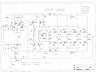


Circuit Schematic

The crystal oscillator is based on a very fast HF transistor, Tl (BFR91), which performs the amplitude modulation. Apart from this there is little to be said about the oscillator except, perhaps, that it is essential to use the correct values for the components surrounding Tl. This is, of course, simply common sense in this sort of HF circuit.

The harmonics generator is formed by two Schottky diodes, Dl and D2. These diodes must switch very quickly in time with the 27 MHz signal so they provide strong harmonics up into the gigahertz range. The modulation depth can be set with Pl, while the oscillators d.c. value can be varied by means of P2. The combination of these two presets enables either positive or negative amplitude modulation to be selected.

This is essential as the harmonics produced vary in this respect. We will discuss the calibration of Pl and P2 later in this article. The power for the circuit can be provided by either an unstabilized 8...30 V or a stabilized 5 V. The latter could be taken from a computers power supply and in this case ICI is not needed.
The printed circuit board for the modulator is only single-sided. The largecopper surface acts as a ground plain.
Parts list
Resistors:
R1, R2 = 4k7
R3, R4 = 56ohm
P1 = 100 ohm preset
P2 = 500 ohm preset
Capacitors:
C1 = 4mf7/16 V
C2= 10p
C3 = 220p
C4 = 47p
C5 = 47n, ceramic
C6 = 100n*
C7 = 330n*
Inductors:
L1, L2 = 3.5 turns of 0.2 mm (SWG 35 or 36) CuL on a ferrite bead of about 3.5 x 3.5 mm
L3 = 1 microH
L4 = 1 turn of 0.8. . .1 mm (SWG 19...21) CuL, air wound with a diameter of 8 mm
Semiconductors:
D1, D2 = 1N6263 (Ambit/Cirkit)
D3 = lN4148
T1 = BFR91 (Ambit/Cirkit)
IC1 = 7805*
Miscellaneous:
X1 = crystal, 27 MHzd(3rd overtone) or other 3rd overtone crystal between 25 and 30 MHz

*= not needed if the circuit is powered from a stabilised 5 V supply 
Read More..

Circuit design tutorial in CircuitMaker 5

In this tutorial we are going to learn how to design and simulate a circuit schematic in CircuitMaker 5. For example we are going to design a 12V to 5V  dc-dc converter circuit diagram.  This is the circuit below that we are going to design. 

Fig-1: 12V to 5V  dc-dc converter circuit diagram


Let’s start design the circuit in circuitmaker 5.


Step-1: Open a new document.
Go to “File>New” as shown below or simply press “CTRL+N” 


This will opened a new workspace named as "UNTITLED.CKT(1)".As shown below...


Step-2: Device Selection.

Click on  “Parts”-(Use to display and select device) tool icon form tool bar. See below…

Or, simply hit on “x” from keyboard.This will bring up  “Device Selection” window.From this window select a 12V DC voltage soure by “Sources>Linear>V source” and change the voltage 10V to 12V as shown below.


After that click on “Select” or press “Enter”.

Now place the symbol where you like by left click on mouse .I placed here..


In the same way add a 78L05 regulator IC symbol. See below… 


And place it in workspace.


As same as add a Diode(shortcut key “d”), Capacitor(shortcut key “c”),and Ground(shortcut key “0”) symbol one after one in the same way and place in workspace(see below). To rotate  any device click on device and press “ALT+R”once or two times or as needed.


To see the circuit in zoom view press F2 . Then you see “Circuit Scale” window, enter a value between 10 to 2000 % that you want to scale (I’m entered 150%). And press “ENTER”.

Now the circuit symbol will larger, now we can design the circuit in circuitmaker 5 easily.


Back to adding schematic symbol.

Now add two “Terminal” (see below...)


Do that two times and then rotate as shown below.


Step-3: Connect the circuit.

Select the “Wire tool” (see below…) 


To connect two pins of two device click to pin(1) and drag until to pin(2). See below…

 
Connect all the pins that are necessary (see Fig:1).

After connect the circuit its looks something like this…


Step-4: Simulate the circuit using circuitmaker simulator.


Don’t worry, this is a simple task. But simulation is necessary for a circuit. To determine that it have any error or it giving us the expected output or not.

Before simulate the circuit we have to confirm that the simulation mode is Analog. To select Analog mode click once on “Digital/Analog” button from toolbar. And then the icon will change. See below...


Now click on “Run/Stop” button from toolbar. See below...


If a confirmation massages box come then select “Yes”.

Then you will see the simulation window. See below...

Showing input value of 12V to 5V  dc-dc converter circuit diagram
Showing output value of 12V to 5V  dc-dc converter circuit diagram
 
Note: If you want to change any parts/device/source value in the circuit, double click on the parts/device/source and enter your value.
Read More..