Showing posts with label using. Show all posts

Tuesday, November 18, 2014

AM Portable Receiver Using ZN414


a AM portable ​​radio receiver using ZN414 IC. The ZN414 ic has now been replaced by the MK484 which is identical in performance and pinout.

Designed around the popular ZN414 IC this receiver covers the range of medium wave band of approximately 550 to 1600 KHz with the values ​​indicated. The condenser coil and tuning can be taken from an old MW radio to save time. The ZN414 IC, has been replaced by the MK484. The integrated circuit is a 3 pin, tuned circuit radio frequency, and incorporates several RF stages, automatic gain control and an AM detector. Its easy to overload and voltage of th IC is critical to success.

In this circuit a small voltage regulator turns on the transistor BC108B, 1N4148 diodes four, 2k7 and 10k resistor and the resistance of pre 820R. The 10k pot control acts as a receptor selectivity for all, control the operating voltage for the ZN414 (or MK484).

The audio amplifier is built on an investment of 741 op-amp amplifier circuit. Additional current pulse is provided by the BC109C / BC179 complementary pair of transistors to drive a 8 ohm speaker. The voltage gain full audio amplifier is around 15. The audio output of the complete receiver is really good and undistorted.
Read More..

Friday, November 14, 2014

100W AUDIO AMPLIFIER USING TDA7294

TDA7294 is an integrated, monolithic, Class AB audio amplifier designed specifically for Hi-Fi applications. The IC has a DMOS output stage and can deliver 100W RMS into an 8Ohm speaker at +/-38V dual supply. The TDA7294 has low noise, low distortion, good ripple rejection and can be operated from a wide range of supply voltages. The IC has built in short circuit protection and thermal shutdown circuitries. The IC is available in multiwatt 15V and multiwatt 15H packages.

Description


In the circuit TDA7294 is configured to provide 100W output power into an 8Ohm loudspeaker at +/- 38V supply. C8 is the input coupling capacitor and the input is applied to the non-inverting input (Pin3) of the IC. C3 and C9 are power supply filter capacitors while C10 and C4 are bypass capacitors. C2 is the bootstrap capacitor. RC network comprising of R1 and C1 improves the high frequency stability of the amplifier and also prevents oscillations. R2 and C6 sets the mute time constant while R3 and C5 sets the standby time constant. S1 and the mute switch and S2 are the standby switch. R5 is the input resistance and the amplifiers input impedance has a direct relationship to its value. R4 and R6 is used for setting type closed loop gain and with the used value, gain is 30dB. C2 is a feedback capacitor and it also provides DC decoupling.

Circuit Diagram


Notes

  • The supply voltage range is +/- 10V to =/-40V DC.
  • Heat sink is required and its thermal resistance should be around 0.038 degree Celsius/Watt.
  • Use an 8 Ohm 150W speaker as the load.
  • For 100W output the supply voltage must be +/-38VDC.
  • The power supply must be well filtered and free of ripples.
  • If ripples are present in the power supply it may cause oscillations.
  • VM = 1.5V is the mute ON threshold and VM=3.5V is the mute OFF threshold.
  • VSTBY = 1.5V is the standby on threshold and VSTBY = 3.5V is the standby OFF threshold.
  • Typical input resistance of TDA7294 is 100KiloOhm.
  • Frequency response is 20Hz to 20KHz.
  • 145 degree Celsius is the threshold for thermal shutdown. Slew rate of TDA7294 is 10V/microsecond and the open loop voltage gain is 80 dB.
  • Quiescent current of TDA7294 is approximately 30mA and its maximum value is 65mA.
Read More..

Thursday, November 13, 2014

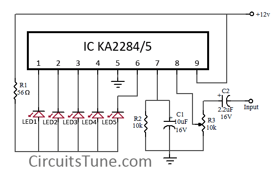
5 LED VU meter circuit diagram using KA2284

This is a simple circuit diagram of 5-LED audio VU meter using IC KA2284/KA2285. The KA2284, KA2285 are monolithic integrated circuit. It is a logarithmic display driver IC. And it is Bar type display driver using 5-Dot LED. The KA2284/KA2285 has a wide range supply voltage capacity of 3.5V-16V, but we recommend to use about a 12VDC power supply.

Circuit Diagram:


KA2284-led
Fig: 5-LED Dot/Bar (VU meter) circuit diagram

Usability of this circuit:

  • AC signal Meter or DC Level meter.
  • Audio VU(Volume Unit) meter in amplifier or such kind of device.
Here IC AN6884 is also can be used instead of KA2284,KA2285. These all are almost same.
Further reading: DOT vs BAR
Read More..

Saturday, November 8, 2014

Battery Discharger Using Discrete Components

The battery discharger published in this website may be improved by adding a Schottky diode (D3). This ensures that a NiCd cell is discharged not to 0.6–0.7 V, but to just under 1 V as recommended by the manufacturers. An additional effect is then that light-emitting diode D2 flashes when the battery connected to the terminals is flat. The circuit in the diagram is based on an astable multivibrator operating at a frequency of about 25 kHz. When transistor T2 conducts, a current flows through inductor L1, whereupon energy is stored in the resulting electromagnetic field. When T2 is cut off, the field collapses, whereupon a counter-emf is produced at a level that exceeds the forward voltage (about 1.6 V) of D2.


A current then flows through the diode so that this lights. Diode D1 prevents the current flowing through R4 and C2. This process is halted only when the battery voltage no longer provides a sufficient base potential for the transistors. In the original circuit, this happened at about 0.65 V. The addition of the forward bias of D3 (about 0.3 V), the final discharge voltage of the battery is raised to 0.9–1.0 V. Additional resistors R5 and R6 ensure that sufficient current flows through D3. When the battery is discharged to the recommended level, it must be removed from the discharger since, in contrast to the original circuit, a small current continues to flow through D3, R2-R3, and R5-R6 until the battery is totally discharged.

The flashing of D2 when the battery is nearing recommended discharge is caused by the increasing internal resistance of the battery lowering the terminal voltage to below the threshold level. If no current flows, the internal resistance is of no consequence since the terminal voltage rises to the threshold voltage by taking some energy from the battery. When the discharge is complete to the recommended level, the LED goes out. It should therefore be noted that the battery is discharged sufficiently when the LED begins to flash.
Read More..

Friday, November 7, 2014

Power Flip Flop Using A Triac

Modern electronics is indispensable for every large model railroad system, and it provides a solution to almost every problem. Although ready-made products are exorbitantly expensive, clever electronics hobbyists try to use a minimum number of components to achieve optimum results together with low costs. This approach can be demonstrated using the rather unusual semiconductor power flip-flop described here. A flip-flop is a toggling circuit with two stable switching states (bistable multivibrator). It maintains its output state even in the absence of an input pulse.

Flip-flops can easily be implemented using triacs if no DC voltage is available. Triacs are also so inexpensive that they are often used by model railway builders as semiconductor power switches. The decisive advantage of triacs is that they are bi-directional, which means they can be triggered during both the positive and the negative half-cycle by applying an AC voltage to the gate electrode (G). The polarity of the trigger voltage is thus irrelevant. Triggering with a DC current is also possible. Figure 1 shows the circuit diagram of such a power flop-flop. A permanent magnet is fitted to the model train, and when it travels from left to right, the magnet switches the flip-flop on and off via reed switches S1 and S2.

Power Flip-Flop Using A Triac  Circuit diagram:

In order for this to work in both directions of travel, another pair of reed switches (S3 and S4) is connected in parallel with S1 and S2. Briefly closing S1 or S3 triggers the triac. The RC network C1/R2, which acts as a phase shifter, maintains the trigger current. The current through R2, C1 and the gate electrode (G) reaches its maximum value when the voltage across the load passes through zero. This causes the triac to be triggered anew for each half-cycle, even though no pulse is present at the gate. It remains triggered until S2 or S4 is closed, which causes it to return to the blocking state.The load can be incandescent lamps in the station area (platform lighting) or a solenoid-operated device, such as a crossing gate. The LED connected across the output (with a rectifier diode) indicates the state of the flip-flop. 

The circuit shown here is designed for use in a model railway system, but there is no reason why it could not be used for other applications. The reed switches can also be replaced by normal pushbutton switches. For the commonly used TIC206D triac, which has a maximum current rating of 4 A, no heat sink is necessary in this application unless a load current exceeding 1 A must be supplied continuously or for an extended period of time. If the switch-on or switch-off pulse proves to be inadequate, the value of electrolytic capacitor C1 must be increased slightly.
Read More..

Thursday, November 6, 2014

Visitor Alarm Circuit Diagram Using IC 555


Description
                  Figure shows the circuit diagram of the Visitor Alarm . Here I have used a LDR and a mono stable Multi Vibrator for making this circuit . When who breaking the LED ray, the LDR has high resistance so the transistor will be OFF and the pin number two of the IC 555 is negative then the IC 555 will be triggering so the output is ON. When who dont breaking the LED ray, the LDR has low resistance so the transistor will be ON and the pin number two of the IC 555 is positive after that the IC 555 doesnt triggering so the output is OFF.

Circuit Idea


Making Of LDR and LED           Cover both items with a black insulation tape. See the below images for further details.
LED
LDR


Arrangement Of LDR and LED


Parts List 
Component No:Value
R110K
R210K
R3680R
R410K
C110MF
C2103pF
Q1BC548
D1White LED Or LASER

LDR
U1NE555
B16V Buzzer
Read More..

Thursday, October 16, 2014

Simple 30 Watt VHF Amplifier by using 2SC1946A

The 30 watt amplifier schematic shown below provides an appropriate power boost with an input of 4 watt up to 6 watts. The circuit is designed to cover 88-108MHz FM Broadcast Band. However, the circuit is very stable at my place and provides a clean-output through seven (7) element Butter-worth low-pass filter.

Circuit Diagram:


Notes:
The heart of the circuit is 2SC1946A VHF RF power transistor. The transistor is specifically designed for operation in frequencies up to 175 MHz, with very good results. As you can see, the power line is well decoupled. The amplifier current can be over 5 amps. All the coils are made from 16gauge laminated wire (or Silver copper wire can do best) and the RFC can be of HF toroid core (as shown in the picture) or 6 holes ferrite bead.C3 and R1 forms snubber circuit while R2 and C6 prevent the amplifier from self-oscillation at VHF, sometimes you need to add 180 ohms in parallel with L7.That will cause the amplifier to dissipate UNDESIRABLE VHF thereby reducing spurious level.


The photo below is 60Watts VHF power amplifier using the above circuit. Two of 2SC1946A transistors are arranged at 90 degrees to each other and their outputs are combined using "Power Combiner Network”. It is quite difficult to combine powers at VHF and UHF bands.

However, I recommend that hobbies should stick to single power design due to its complicity and large rate of INTERFERENCE. (in attempt to go for double transistors which involves power combiner network). Since the two amplifiers are operating in different phase (out of phase).

Tuning:
Tuning of the amplifier is not hard at all. You just have to connect the output to a good antenna with a transmission line (RG214) of 50 ohms. First match the output network, and then do the same to the input network for a maximum power output. By way of adjustment, you can increase the output at its operating frequency.
Read More..

Tuesday, September 16, 2014

On Demand WC Fan Using 555

In most WCs with an extractor the fan is connected to the lighting schema and is switched on and off either in sympathy with the light or with a short delay. Since toilets are sometimes used for washing the hands or just for a quick look in the mirror, it is not always necessary to change the air in the smallest room in the house. The following schema automatically determines whether there really is any need to run the fan and reacts appropriately. No odour sensor is needed: we just employ a small contact that detects when and for how long the toilet seat lid is lifted.

 On-Demand WC Fan Using 555 schema diagram


If the seat lid is left up for at least some presettable minimum time t1, the fan is set running for another presettable time t2. In the example shown the contact is made using a small magnet on the lid and a reed switch mounted on the cistern. The rest is straightforward: IC2, the familiar 555, forms a timer whose period can be adjusted up to approximately 10 to 12 minutes using P2. This determines the fan running time. There are three CMOS NAND gates (type 4093) between the reed switch and the timer input which generate the required trigger signal. When the lid is in the ‘up’ position the reed switch is closed.

Capacitor C1 charges through P1 until it reaches the point where the output of IC1a switches from logic 1 to logic 0. The output of IC1b then goes to logic 1. The edge of the 0-1 transition, passed through the RC network formed by C2 and R2, results in the output of IC1c going to logic 0 for a second. This is taken to the trigger input on pin 2 of timer IC2, which in turn switches on the relay which causes the fan to run for the period of time determined by P2. The schema is powered from a small transformer with a secondary winding delivering between approximately 8 V and 10 V. Do not forget to include a suitable fuse on the primary side.

The schema around IC1b and IC1c ensures that the fan does not run continuously if the toilet seat lid is left up for an extended period. The time constant of P1 and C1 is set so that the fan does not run as a result of lavatorial transactions of a more minor nature, where the lid is opened and then closed shortly afterwards, before C1 has a chance to charge sufficiently to trigger the schema.


Circuit Source: CircuitsProject
Read More..

Monday, September 15, 2014

SP LED Flashlight Using Supercapacitor

Bored of joking with capacitors? Then its time for you to maneuver on to super-capacitors. These have huge storage capabilities. during this article you may conclude the way to build atiny low LED flashlight using supercapacitors.

The most disadvantage of capacitors is their giant voltage drop. For this project, a minimum voltage of two volts is needed to light-weight the LED. As a result, the “Joule Thief” style would be incorporated here. Using this, a AA battery is used to light-weight an LED until its fully discharged.
 during this case, a supercapacitor would be taking the place of the battery. Here an LED is employed to perform the operate of a diode. This ensures that theres sufficient voltage across the LED.

 the necessities of the project are listed below:
White LED
Super capacitor (10F, 2.7 V)
Transistor
Torus
1 k ohm resistor
Wires
Breadboard
The torus and therefore the transistor used here comes from an energy-saving lamp HS. Care ought to be taken whereas removing this from the lamp as a breakage may lead to the discharge of the mercury vapors. A lamp load along side a USB port is added to the schema. This makes it compatible with a computer or a automotive radio.


A couple of precautions got to be taken whereas constructing the schema. The USB port mustnt be supplied with excess power. The capacitor doesnt stand up to a high voltage and hence a zener diode is connected in parallel to handle the high voltage. The diode protects the capacitor when the voltage exceeds an explicit price.
Read More..

Friday, September 12, 2014

200 Watt Amplifier Wiring diagram Schematic using TDA2030

This is a 200 Watt Amplifier Circuit Diagram that uses a TDA2030 IC which is an audio power amplifier 200 watt low cost. The 200 watts can be achieved with a load impedance of 4 ohms. The TDA2030 can typically provide up to 14 watts into a 4 ohm load, but if used in bridge mode and we use some cheap power transistors we can get to 200 watt. The design of this amplifier schema 200 watt audio is very simple and requires few external components. For best performance, you can use a source of 28 volts (+ / - 14 volts), not more than 44 volts (+ / - 20 volts).

 As you can see in the diagram, for this power amplifier schema you need high capacity capacitors and a power supply high current. All transistors and ICS should be mounted on a heat sink to prevent damage by temperature. For small value resistors (1 ohm, 2.2 ohm) resistors use 2-5 watts.

 200 Watt Amplifier Circuit Diagram using TDA2030

200

Read More..

Thursday, September 11, 2014

How to Using Diodes as a photosensor Circuit diagram

Using

A photodiode is a PN junction or PIN structure that when light reaches the junction, it excites an electron thereby creating a free electron positively charged. This mechanism is also known as the photoelectric effect, common in transistors, diodes and ICs are made ​​of semiconductors, and contain PN junctions. Almost all of the potentially active constituents are a photodiode and may be used as a photosensor. The PN junction needs to be exposed to light, so to use a semiconductor diode as a light bulb must have a transparent glass, these diodes with these characteristics can be used to measure the light intensity.


 Circuit diagram of a light intensity meter with diode.

Circuit


a test schema diode light sensor

List of components:
D1 1n148 or any other photo-sensitive element
T1, T2 BC548 or similar
C1 680n
R1 2M

Above this schema that is very popular, it works with LEDs, photodiodes and photo-resistors. V is a voltmeter which can be a multimeter.

sourced by www.diagramstream.blogspot.com
Read More..

Wednesday, September 10, 2014

Simple Solar charger circuit project using transistors

A very simple solar charger schema project can be designed using few external electronic parts . This simple solar charger schema is capable of handling charge currents of up to 1A. Alternate component values are given in the figure for lower current applications.

Circuit diagram:
12V-SLA-chargher Solar charger schema project using transistors schema diagram

The only adjustment is the voltage trip point when the current is shunted through the transistor and load resistor. This should be set with a fully charged battery. As the transistor and R3 have the entire panel’s output across them when the battery is fully charged, all of the current from the panel will be going through R3 and the Darlington transistor TIP112, so these must be well heat sunk. Adjust R1 for the trip point, usually 14.4 V – 15 V for a 12 V SLA or a 12 V Ni-Cd battery.
Read More..

Saturday, September 6, 2014

3 Channels Audio Splitter Amplifier Wiring diagram Schematic using TL084

This is the schematic diagram of 3 channels audio splitter amplifier schema which built using op-amp IC TL084. The 3 channels amplifier output distribution applies a single TL084.

  3 Channels Audio Splitter Amplifier Circuit Diagram

 3 channels audio splitter amplifier circuit diagram


The very first step is to capacitive coupling having a p. 1.0 ~ electrolytic capacitor. The entries are railways Vee Y2 or 4.5 V. This enables working with an individual 9V power source. A voltage gain of 10 (1 M?/100 Kohm) is obtained in the first stage, as well as the other three floors are connected as a unity gain voltage followers. Every single output stage drives independently through an amplifier output 50 pF capacitor towards the resistance of 5.1 k ohm load. The response range is flat from 10 Hz to 30 kHz.
Read More..

Wednesday, September 3, 2014

Build a Toggle Touch Switch Using Two Inverter Gates

We  can make a simple touch switch using only two inverter gates, two resistors, and two capacitors. The schematic diagram of the schema is shown in the figure below. At power up, the output (of U1A) will be high, and the inverting output will be low because U1A gate will be triggered to ground level by C2. After triggered, the low level of U1A input is maintained by U1B output via R2.

Toggle Touch Switch Using Two Inverter Gates Circuit Diagram


Toggle
If we touch the pad at this condition, where the output is high, then the U1A input will go high because we “short” the voltage of C1 to the input pin, and the low level previously caused by low level of U1B output voltage connected via R2 can’t be maintained because our skin resistance is much lower than 10M.

After U1A input goes high then U1A output will go low, and now U1B will go high to maintain high voltage level of U1A via R2, so we can release our finger without loosing the last state. Touching the pad again after we release our previous touching will toggle the output as the condition is reversed.

After we touch the pad, we have to release before 1 second (R2C2 time constant) elapsed. If we touch the pad longer than R2C2 time constant then  the output will oscillate (about 1 Hz).


Read More..

Thursday, August 28, 2014

Voltage Controlled Attenuator VC Using FET

Build a Voltage-Controlled Attenuator VC Using FET. Using the schema shown in the schematic diagram below, we can control the low-level audio signals with ±3V variable DC voltage. This attenuator schema uses a field effect transistor (FET) to shunt the signal to ground. The R2 is used to control the output level (the attenuation level), but you can use other source of voltage signal to control the grid of the FET, such as DAC output, just remember that this voltage is a negative going signal (you can use with DAC which uses symmetric power supply system). The minimum output of this schema is when gate bias is zero. When the gate bias is set close to pinchoff value, the schema will produce maximum output with value that equal to input level. Here is the schematic diagram of the schema:

Voltage-Controlled Attenuator VC Using FET Circuit Diagram


Build

Read More..

Wednesday, August 27, 2014

Touch Switch using NE555

The series of touch switch or touch switch is built by IC NE555, a series of touch switches can be used to turn on lights, alarms or other electronic equipment.
This circuit uses 2 pieces of metal plate media as touch, MP1 (Metal Plate 1) and MP2 (Metal Plate 2). Touch switch circuit is equipped with a visual LED indicator for relay status (load active). To enable (Relay ON) can be done by touching the surface of MP1 and to turn it off by touching the surface of the MP2. MP1 and MP2 in touch this switch can use a small piece of copper (diameter 5mm) was enough.


Touch Switch series with NE555.
555


Component List 555 touch Switch
R1 = 3.3M
R2 = 3.3M
R3 = 10K
R4 = 1K
C1 = 10nF-63V
D1 = 1N4007
D2 = Red LED
Q1 = BC547
IC1 = NE555
RL1 = 12V Relay
Read More..

Thursday, August 21, 2014

Build a VHF UHF Low Noise Amplifiers using MAX2664 MAX2665

A very simple VHF UHF Low-Noise amplifiers schema can be designed using the MAX2664 and MAX2665 ultra-compact LNAs for VHF UHF applications.These devices incorporate a broadband LNA with an integrated bypass switch. The MAX2664 covers the UHF frequency range from 470MHz to 860MHz, and the MAX2665 covers the VHF frequency range from 75MHz to 230MHz. Each device has a zero-power bypass mode for improved high-signal-level handling conditions.

VHF UHF Low-Noise Amplifiers using MAX2664 MAX2665  


 Both ICs has a high gain around 15dB and require a single power supply , that can provide an output voltage between 2.4 to 3.5 volts .VHF UHF Low-Noise amplifiers has a very low current consumption of 3.3 mA and can be used in applications like : Smartphones/Handsets , MP3 Players , Home Audio/Video and other portable navigation devices .
Read More..

Wednesday, August 20, 2014

Simple Battery Charger using LM350

Simple

The schematic diagram can be used for charging the 12V lead acid batteries.

The schema is designed as a constant voltage source with a negative temperature coefficient. The transistor Q1 (BD 140) is used as the temperature sensor. The transistor Q2 is used to prevent the battery from discharging through R1 when the mains power is not available. The schema is designed based on the voltage regulator IC LM350. The output voltage of the charger can be adjusted between 13-15 V by varying the POT R6.

The LM350 will try to keep the voltage drop between its input pin and the output pin at a constant value of 1.25V. So there will be a constant current flow through the resistor R1. Q1 act here as a temperature sensor with the help of components R6/R3/R4 which more or less control the base current of Q1. As the emitter/base connection of transitor Q1, just like any other semiconductor, contains a temperature coefficient of -2mV/°C, the output voltage will also show a negative temperature coefficient. That one is only a factor of 4 larger, because of the variation of the emitter/basis of Q1 multiplied by the division factor of P1/R3/R4. This results in approximately -8mV/°C. The LED will glow whenever the mains power is available.

The transistor Q1 must be placed as close as possible to the battery.
Use a 20 to 30 V / 3A DC power supply for powering the schema.
This schema is not possible for charging GEL type batteries as it draw large amounts of current.

Here the LM350 pin layout:
 here the lm350 pin layout
Read More..

Monday, August 11, 2014

Intruder Detector Using Laser Torch

Here is a simple, low-cost intruder detector that uses an invisible laser beam to detect the intruder. The laser beam is produced using a 3V DC or 4.5V DC laser pointer or torch that is available in the market. The 3V DC or 4.5V DC power supply for the laser transmitter can also be given using a bridger ectifier or full-wave rectifier.

Fig. 1 shows the block diagram of the complete unit comprising the transmitter and receiver sections. The laser beam from the transmitter after reflection from various mirrors (M1 through M6, as shown in Fig. 1) is made to fall on the photodetector in the receiver schema.


Fig. 1: Block diagram of intruder detector using laser torch

Fig. 1: Block diagram of intruder detector using laser torch

Once the laser beam is positioned, the receiver schema is powered by closing switch S. An alarm unit operating on 230V AC is connected to the relay RL in the receiver schema.

When an intruder interrupts the path of the beam or switches off the laser torch, the alarm unit becomes activated. The alarm unit remains activated until reset switch S is opened. To activate the alarm schema again, reset switch S should be closed. The total distance travelled by the laser beam should be less than 800 m for 4.5V laser torch and 500 m for 3V laser torch.

The schema of the receiver is shown in Fig. 2. When reset switch S is closed, the schema is powered on. As the laser beam falls on the photodetector, transistor T (BC547) conducts, resulting in the collector being pulled down to ground potential. Thus no current flows to the gate of the SCR and it remains off.

Fig. 2: Receiver schema

Fig. 2: Receiver schema

Once the path of the laser beam is interrupted, the base current of the transistor becomes very low and the transistor is driven to cut-off. Now the current starts to flow through resistor R1 and to the gate of SCR. Hence the SCR is fired and it begins to conduct. Thus relay RL connected to the anode of SCR is switched on and the alarm is activated. The alarm sounds until reset switch S is opened to turn off power to the schema.

EFY Lab note. We tested the schema using only one mirror and found its range to be 25-30 metres. The range depends on the intensity of laser beam falling on the photodetector.

The schema (excluding laser torch and mirrors) costs around Rs 100.


Sourced by : EFY Author : G. Susinder Rajan
Read More..

Saturday, August 9, 2014

Battery charger using LM350


This is very useful schema for the vehicle owners.Because most of time they have to bring their heavy 12v battery hear and there.now you dont want to do that.because you can build your own 12v charger


Notes

Use a 20 to 30 V / 3A DC power supply for powering the schema.

This schema is not possible for charging GEL type batteries as it draw large amounts of current.
Read More..