Showing posts with label build. Show all posts
Showing posts with label build. Show all posts
Thursday, October 16, 2014
Build a Compressor Circuit with 570 571 Compandor IC
Compressor Circuit with 570/571 Compandor IC circuit provide high gain for low amplitude input and provide low gain for high amplitude input. This action, in effect, produce a nearly constant amplitude even though the input has very high dynamic range (very high amplitude variation from time to time). The action of compression like this is needed in some situation, such as in maximizing modulation depth in broadcasting, or sustaining electric guitar signal which has very high variation between the plucking time and fading out. The following circuit has complementary input/output characteristic and unity gain at 0.775 VRMS input. Voltage gain through compressor is square root of 0.7/Vin. Vin is average input voltage. This circuit uses Signetics dual channel compandor IC. 570 has lower inherent distortion and higher supply voltage range (6-24 V) than 571 (6-18 V).
Compressor Circuit with 570/571


Wednesday, October 15, 2014
Build an Alarm Control Keypad Circuit Diagram
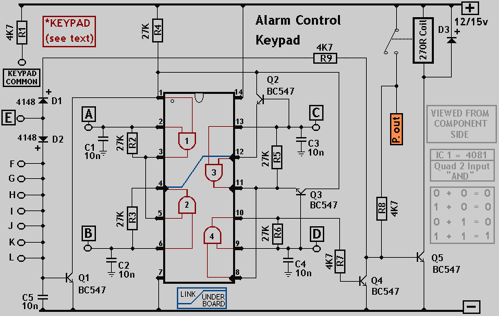
The IC is a quad 2 input “AND” gate, a CMOS 4081. These gatesonly produce a HIGH output, when BOTH the inputs are HIGH. Whenthe key wired to `E` is pressed, current through R1 and D1switches Q5 on. The relay energises; and Q5 is `latched on` byR8. Thus, the Alarm is set by pressing a single key, say one ofthe tw1o non-numeric symbols.The alarm will switch off when the 4 keys connected to“A,B,C,D” are pushed in the right order. The circuit worksbecause each gate `Stands` upon its predecessor.If any key otherthan the correct key is pushed, then gate 1 is knocked out of thestack, and the code entry fails.
Pin 1 is held high by R4. This`Enables` gate 1; and when button `A` is pressed, theoutput at pin 3 will go high. This output does tw1o jobs.It locksitself `ON` through R2 and it `Enables` gate 2, by taking pin 5,high. Now, if `B` is pressed, the output of gate 2, at pin 4will go high. This output does tw1o jobs. It locks itself `ON`through R3 and it `Enables` gate 3 by taking pin 12 high.Now, if `C` is pressed, the output of gate 3 will lock itself`ON` through R5 and, by taking pin 8 high, `Enable` gate 4.Pressing `D` causes gate 4 to do the same thing; only this timeits output, at pin 10, turns Q4 `ON`.
This takes the base of Q5to ground, switching it off and letting the relay drop out. Thisswitches the alarm off.Any keys not connected to `A B C D E` are wired to the base ofQ1. Whenever `E` or one of these other keys is pressed, pin 1 istaken low and the circuit is reset. In addition, if `C` or `D`is pressed out of sequence, then Q2 or Q3 will take pin 1 low andthe circuit will reset. Thus nothing happens until `A` ispressed. Then if any key other than `B` is pressed, the circuitwill reset.Similarly, after `B`, if any key other than `C` is pressed,the circuit will reset. The same reasoning also applies to `D`.The Keypad needs to be the kind with a common terminal and aseparate connection to each key. On a 12 key pad, look for 13terminals. The matrix type with 7 terminals will NOT do.
Wire thecommon to R1 and your chosen code to `A B C D`. Wire `E` to thekey you want to use to switch the alarm on. All the rest go tothe base of Q1.The diagram should give you a rough guide to the layout of thecomponents, if you are using a strip board. The code you choosecan include the non-numeric symbols. In fact, you do not have touse a numeric keypad at all, or you could make your own keypad.I haven`t calculated the number of combinations of codesavailable, but it should be in excess of 10 000 with a 12 keypad; and, after all, any potential intruder will be ignorant ofthe circuit`s limitations. Of Course, if you must have a moresecure code, I can think of no reason why you shouldn`t addanother 4081 and continue the process of enabling subsequentgates. Or you could simply use a bigger keypad with more “WRONG”keys.Any small audio transistors should do.
The 27k resistors couldbe replaced with values up to 100k. And the only requirementsfor the 4k7 resistors is that they protect the junctions whileproviding enough current to turn the transistors fully on.Capacitors (C1 C2 C3 C4 C5) are there to slow response timeand overcome any contact bounce. They are probably unnecessary.
Alarm Control Keypad Circuit Diagram
Saturday, September 13, 2014
Build a Beacon Transmitter Wiring diagram Schematic
Build a Beacon Transmitter Circuit Diagram. This Beacon Transmitter Circuit Diagram can be used for transmitter hunts, for remote key finding, or for radio telemetry in model rockets. It can be tuned to the two meter band or other VHF bands by charging Cl and Ll. 11 is four turns of #20 enameled wire airwound, 0.25 inch in diameter (use a drill bit), 0.2 inch long, centertapped.
The antenna can be 18 inches of any type of wire. IC2 functions as an audio oscillator that is turned on and off by IC1 about once per second. The range of the transmitter is several hundred yards.
Beacon Transmitter Circuit Diagram
Friday, September 12, 2014
Build a Circuit indication for RF Output Transmitters On Air
This is an On Air indicator, ie an indicator schema dr RF transmission, very simple and useful for those who like RF. This schema detects the RF output using a visual indicator, but with some modifications, the LED may be replaced by a relay or any other system that want to trigger when the transmitter is switched on. The output of the transmitter or other RF generator must be connected to this RF input schema.
Simple Circuit indication for RF Output Transmitters
List of components
Resistor R1 560Ω eighth
Capacitor C1 330pF disc
C2 Capacitor 0.1μF disc
Diode D1 1N34 or 1N60
D2 LED
Transistor Q1 2N3904 or equivalent
If you liked this article,Take a few Seconds to Share this and leave comments
Monday, September 8, 2014
Build a 5V 0 5A Power Supply Wiring diagram Schematic
The 5V 0.5A Power Supply Circuit Diagram is essentially a constant source modified by the feedback components R2 and R3 to give a constant voltage output. The output of the ZN424E need only be 2 volts above the negative rail, by placing the load in the collector of the output transistor Tr2. The current 5V 0.5A Power Supply Circuit Diagram is achieved by Trl and R5. This simple schema has the following performance characteristics: Output noise and ripple (full load) = 1 mV rms. Load regulation (0 to 0 A) = 0%. Temperature coefficient — ± 100 ppm/°C. Current limit = 05 A.
5V 0.5A Power Supply Circuit Diagram
Wednesday, September 3, 2014
Build a High input comparator Wiring diagram Schematic
This is a simple High input comparator Circuit Diagram. The inputs of an ideal comparator exhibit infinitely high input resistance, and thus no current flows into its inputs. The schema uses both halves of the CA3290 BiMOS dual voltage comparator. The LED will be turned `ON` whenever the input signal is above the lower limit (VL) but below the upper limit (Vy).
High input comparator Circuit Diagram
Build a Toggle Touch Switch Using Two Inverter Gates
We can make a simple touch switch using only two inverter gates, two resistors, and two capacitors. The schematic diagram of the schema is shown in the figure below. At power up, the output (of U1A) will be high, and the inverting output will be low because U1A gate will be triggered to ground level by C2. After triggered, the low level of U1A input is maintained by U1B output via R2.
Toggle Touch Switch Using Two Inverter Gates Circuit Diagram
After U1A input goes high then U1A output will go low, and now U1B will go high to maintain high voltage level of U1A via R2, so we can release our finger without loosing the last state. Touching the pad again after we release our previous touching will toggle the output as the condition is reversed.
After we touch the pad, we have to release before 1 second (R2C2 time constant) elapsed. If we touch the pad longer than R2C2 time constant then the output will oscillate (about 1 Hz).
Sunday, August 31, 2014
Build a Diode Cmos Stabilizer Wiring diagram Schematic
The simple diode network can stabilize the voltage supplied to CMOS schemary from a battery. D1 and D2 must have a combined forward-voltage drop of about 1.5 V. And D3 is an LED with a forward-voltage drop of about 1.7 V. The table shows the network`s output voltage as the battery`s voltage declines.
Diode Cmos Stabilizer Circuit Diagram
Saturday, August 30, 2014
Build 20W MOSFET Power Amplifier Circuit with IFR9520 IFR520
As we are like to show you about audio and sound schema ,I found the schema which is good one for power amplifier with one MOSFET.
The output power of an operational amplifier is often increased by a complementary emiter follower.
20W power amp MOSFET
It can also be done with a MOSFET,but it is not a good idea to connect such a device as a complementary souce follower because the maximum output voltage of the opamp is then reduced appreciably by the gate-source control voltage of the MOSFET ,which can be a couple of volts.
Another approach is to connect two MOSFETs as a complementary drain follower.The (alternating) output current provided by the MOSFETs is limited by the level of the supply voltages and the saturateion voltages of T3 and T4 Resistor R8,together with R9,provides feedback for both the opamp and MOSFETs .
The open-loop amplification of the opampis,therefore,increased by (1+R8/R9).the closed-loop amplification of the complete amplifier is (1+R3/R2).
The current source formed by T1 and T2 is required for arreanging the quiescent current of T3 and T4 at 50 mA.The values of resistors R4 and R5 are such that,without the current source the voltage drop across the resistor resulting from the direct current through the opamp is not sufficient to switch on T3 and T4 .with the current source,and depending on the setting of P1,the voltages across R4 and R5 rise,which increases the quiescent current through T3 and T4.
In view of the temperature dependence of the quiescent current,T2 must be mounted on the common heat sink(c. 5 K/W) of the MOSFETs.
The output power is not less than 20 W into 8 ohm,at which level the harmonic distortion amounts to 0.075 per cent at 100 Hz to 0,135 per cent at 10 kHz.
Saturday, August 23, 2014
Build a Heavy Duty Battery Charger Wiring diagram Schematic
How to Build a Heavy Duty Battery Charger Circuit Diagram. Operation amplifier A1 directly drives the VN64GA with the error signal to control the output voltage. Peak rectifier Dl, CI supplies error amplifier A1 and the reference zener. This extra drive voltage must exceed its source voltage by several volts for the VN64GA to pass full load current.
The output voltage is pulsating dc which is quite satisfactory for battery charging. To convert the system to a regulated dc supply, capacitor C2 is increased and another electrolytic capacitor is added across the load. The response time is very fast, being determined by the op-amp.
Heavy Duty Battery Charger Circuit Diagram
The 2N4400 current limiter schema prevents the output current from exceeding 4.5 A. However, maintaining a shorted condition for more than a second will cause the VN64GA to exceed its temperature ratings. A generous heat sink, on the order of 1°C/W, must be used.
Thursday, August 21, 2014
Build a VHF UHF Low Noise Amplifiers using MAX2664 MAX2665
A very simple VHF UHF Low-Noise amplifiers schema can be designed using the MAX2664 and MAX2665 ultra-compact LNAs for VHF UHF applications.These devices incorporate a broadband LNA with an integrated bypass switch. The MAX2664 covers the UHF frequency range from 470MHz to 860MHz, and the MAX2665 covers the VHF frequency range from 75MHz to 230MHz. Each device has a zero-power bypass mode for improved high-signal-level handling conditions.
VHF UHF Low-Noise Amplifiers using MAX2664 MAX2665

Both ICs has a high gain around 15dB and require a single power supply , that can provide an output voltage between 2.4 to 3.5 volts .VHF UHF Low-Noise amplifiers has a very low current consumption of 3.3 mA and can be used in applications like : Smartphones/Handsets , MP3 Players , Home Audio/Video and other portable navigation devices .
Thursday, August 14, 2014
Build 16 Stage Bi Directional LED Sequencer
The bi-directional sequencer uses a 4 bit binary up/down counter (CD4516) and two "1 of 8 line decoders" (74HC138 or 74HCT138) to generate the popular "Night Rider" display. A Schmitt Trigger oscillator provides the clock signal for the counter and the rate can be adjusted with the 500K pot. Two additional Schmitt Trigger inverters are used as a SET/RESET latch to control the counting direction (up or down). Be sure to use the 74HC14 and not the 74HCT14, the 74HCT14 may not work due to the low TTL input trigger level. When the highest count is reached (1111) the low output at pin 7 sets the latch so that the UP/DOWN input to the counter goes low and causes the counter to begin decrementing.
When the lowest count is reached (0000) the latch is reset (high) so that the counter will begin incrementing on the next rising clock edge. The three lowest counter bits (Q0, Q1, Q2) are connected to both decoders in parallel and the highest bit Q3 is used to select the appropriate decoder. The schema can be used to drive 12 volt/25 watt lamps with the addition of two transistors per lamp as shown below in the section below titled "Interfacing 5 volt CMOS to 12 volt loads"
Circuit diagram

schema from Link
Subscribe to:
Posts (Atom)