Showing posts with label with. Show all posts

Monday, January 26, 2015

Stereo Preamplifier With Bass Boost

This preamplifier was designed to cope with CD players, tuners, tape recorders etc., providing an ac voltage gain of 4, in order to drive less sensitive power amplifiers. As modern Hi-Fi home equipment is frequently fitted with small loudspeaker cabinets, the bass frequency range is rather sacrificed. This circuit features also a bass-boost, in order to overcome this problem. You can use a variable resistor to set the bass-boost from 0 to a maximum of +16dB @ 30Hz. If a fixed, maximum boost value is needed, the variable resistor can be omitted and substituted by a switch.

 Stereo Preamplifier With Bass Boost Circuit diagram:

Parts:
P1 = 10K
P2 = 100K
R1 = 100K
R2 = 100K
R3 = 15K
R4 = 10K
R5 = 22K
R6 = 15K
R7 = 1K
R8 = 470R
C1 = 2.2uF-25v
C2 = 2.2uF-25v
C3 = 470uF-35v
C4 = 1uF-35V
C5 = 2.2uF-25v
C6 = 47nF-63v
C7 = 22uF-25v
IC1 = TL072, Opamp
SW1 = DPST Switch
Notes:
  • Schematic shows left channel only, but R1, R2, R3 and C1, C2, C3 are common to both channels.
  • For stereo operation P1, P2 (or SW1), R4, R5, R6, R7, R8 and C4, C5, C6, C7 must be doubled.
  • Numbers in parentheses show IC1 right channel pin connections.
  • A log type for P2 ensures a more linear regulation of bass-boost.
  • Needing a simple boost-in boost-out operation, P2 must be omitted and SW1 added as shown in the diagram.
  • For stereo operation SW1 must be a DPST type.
  • Please note that, using SW1, the boost is on when the switch is open, and off when the switch is closed.
 
Read More..

Wednesday, November 19, 2014

120W amplifier with LM12

This is power amplifier with basic amplifiy on IC LM12.

Read More..

Tuesday, November 18, 2014

Power Supply with Z2C Tubes

Power supply with Z2C tubes are designed specifically to provide power supply voltage to the EL-34 tube amplifier push-pull in the previous article. Power supply with Z2C tube to tube power amplifier is made with a tube rectifier Z2C. Just as the power supply for power amplifier tube before, the power supply is also using 3-level filter with electrolytic capacitors. Circuit power supply with tube rectifier Z2C can give +210 VDC output voltage.


Power supply with Z2C tube is a power supply that can be used as a replacement power supply for power amplifier with a diode tube
Read More..

Monday, November 17, 2014

10W Audio Amplifier with Bass boost


This Audio Amplifier design is based on the audio amplifier 18 watts, and was developed primarily to meet the requests of correspondents unable to locate the chip TLE2141C. It uses the NE5532 Dual IC wide, but obviously, its power output will be written in the 9.5 - 11.5W range, as the supply rails can not exceed ± 18V.

As amplifiers of this type are often used to drive small loudspeaker cabinets, the bass frequency range is rather sacrificed. Therefore, a Bass Boost control was inserted in the amplifier feedback loop, in order to overcome this problem, without loss of quality. The low elevation curve can reach a maximum of 16.4 dB @ 50Hz. In any case, even when the bass control is turned fully counterclockwise, the amplifiers frequency response curve shows a gentle rise: 0.8 dB at 400 Hz, 4.7 dB at 100 Hz and 6 dB at 50 Hz (referred to 1 kHz).
Read More..

Pulse generator circuit with Logic Gate

Pulse generator circuit above is a pulse generator that uses logic gates. There are so many types and variations that can generate a series of pulses.
The simplest is the use of transistors or often called a flip-flop. There also are using integrated circuit such as IC 555. Theres more to exploit the resonance of the capacitor and inductor relationship as oscillators. To be sure whatever form and whatever the circuit components used must be able to generate electric waves which have a peak voltage (logic 1) and valleys (logic 0) is continuous.


Any variation of pulse generator circuit design has advantages and disadvantages of each, just how your decision for the appropriate circuit. For example to create a clock signal for a simple utility that you can only take advantage of the transistor but if you need a more accurate clock signal and form a perfect balance you can use IC Astable or logic gates. Or perhaps you need a signal with very high frequency (up to MHz) you can use a combination of inductor, resistor and capacitor.

Frequency value of the pulse generator circuit gate above is determined by the value kapaitor C2, R2, R3 and VR2. The greater the value of these components will lower the frequency and vice versa. Actually nothing is difficult to make a series of pulse generators, almost all time-based series is utilizing the nature of the charge and discharge capacitor. Therefore, like any form of variations in pulse generator circuit, always have a larger capacitor value will make the frequency produced smaller or longer periods of time, sedangkaan smaller capacitor values ​​will result in greater output frequency.
Read More..

Simple FM transmitter with 2N3904

In this section discuss about the series of mini fm transmitter, with broadcast coverage of about 300-400 meters. when using a 9 volt working voltage, the transmit power of about 300 meters and when using the working voltage 12 volts, the range of about 400-450 meters, depending on the antenna you use.

This scheme of simple fm transmitter

For L1 and L2 windings 5 times the wrap, you can use a pen to fill melilitnya so neat and after lepaslah content of these pens. C5 is used for placement of broadcasting frequencies, can be tuned between 88-108 mhz, to reach further use steering antenna or Yagi antenna.

Part List
C1 = 0.001uF
C2 = 5.6pF
C3 = 10uF
C4 = 10uF
C5 = 3 - 18pF Adjustable capacitor
R1 = 270R
R2 = 4.7K
R3 = 10K
R4 = 100K
R5 = 4.7K
R6 = 4.7K
Q1 = 2N2222A
Q2 = 2N3904
L1 = 5 turn
L2 = 5 turn
Read More..

Wednesday, November 12, 2014

VHF RF Single Chip Preamplifier circuit with explanation

Here is a high performance RF amplifier for the entire VHF broadcast and PMR band (100-175 MHz) which can be successfully built without any special test equipment. The grounded-gate configuration is inherently stable without any neutralization if appropriate PCB layout techniques are employed. The performance of the amplifier is quite good.
The noise figure is below 2 dB and the gain is over 13 dB. The low noise figure and good gain will help car radios or home stereo receivers pick up the lower-power local or campus radio stations, or distant amateur VHF stations in the 2-metres band. Due to the so-called threshold effect, FM receivers loose signals abruptly so if your favourite station fades in and out as you drive, this amplifier can cause a dramatic improvement.
The MAX2633 is a low-voltage, low-noise amplifier for use from VHF to SHF frequencies. Operating from a single +2.7 V to +5.5V supply, it has a virtually flat gain response to 900 MHz. Its low noise figure and low supply current makes it ideal for RF receive, buffer and transmit applications. The MAX2633 is biased internally and has a user-selectable supply current, which can be adjusted by adding a single external resistor (here, R1). This circuit draws only 3 mA current.

VHF RF preamplifier circuit diagram

Besides a single bias resistor, the only external components needed for the MAX2630 family of RF amplifiers are input and output blocking capacitors, C1 and C3, and a VCC bypass capacitor, C2. The coupling capacitors must be large enough to contribute negligible reactance in a 50-Ω system at the lowest operating frequency. Use the following equation to calculate their minimum value:
Cc = 53000/ flow [pF]
Read More..

Tuesday, November 11, 2014

PIC 12F629 – 12F675 based Astable Timer circuit with explanation


This software functions as a long period astable mutivibrator. The mark and space period can be set from 1 second up to a maximum 65535 seconds (18h12m15s). Using the internal 4Mhz RC oscillator delays with an accuracy of 99% or better can be achieved The code also implements an edge triggered reset and an active low hold function. The reset edge can be configured for rising or falling edge. The hold function is active low and stretches the timed period for as long as the hold input is held low. In addition to this up to 128 mark/space time pairs can be used which are executed sequentially allowing complex pulse trains to be generated. 
Read More..

Thursday, October 16, 2014

Build a Compressor Circuit with 570 571 Compandor IC

Compressor Circuit with 570/571 Compandor IC circuit provide high gain for low amplitude input and provide low gain for high amplitude input. This action, in effect, produce a nearly constant amplitude even though the input has very high dynamic range (very high amplitude variation from time to time). The action of compression like this is needed in some situation, such as in maximizing modulation depth in broadcasting, or sustaining electric guitar signal which has very high variation between the plucking time and fading out.  The following circuit has complementary input/output characteristic and unity gain at 0.775 VRMS input. Voltage gain through compressor is square root of 0.7/Vin. Vin is average input voltage. This circuit  uses Signetics dual channel compandor IC.  570 has lower inherent distortion and higher supply voltage range (6-24 V) than 571 (6-18 V).

Compressor Circuit with 570/571 


Read More..

Thursday, September 18, 2014

Simple Theremin with Inverter Gates Wiring diagram Schematic

This simple but complete Theremin with Inverter Gates is constructed using only two inverter chip plus one regulator IC. This Theremin schema consist of five functional blocks: power supply regulator, hand controlled oscillator, null oscillator, mixer, and filter. Here is the complete schematic diagram.

Theremin with Inverter Gates schematic diagram


Build


Voltage Regulator and Circuit Protector
The power supply regulator consist of LP2950 regulator IC, which stabilize the voltage from battery to 5V. You can use more popular 7805 IC for this, but since the power consumption of this Theremin schema is very small, then you can use 78L05 which is smaller.  CR1 diode is used to protect from inappropriate battery polarity,  shorting the battery voltage together with R8 100 Ohm resistor which prevent the large current when the battery is installed in wrong direction. Although the inverter chip will work well for 9V battery, there is a benefit of using voltage regulation to regulate the battery voltage at lower voltage level, that the voltage will remain constant for until the end of battery life. This will avoid frequency drift of the Theremin’s null oscillator  which should be carefully adjusted to zero the output frequency, which can be affected by the supply  voltage.

Hand Controlled Oscillator
The hand proximity sensor is an oscillator which has antenna extension which shift the capacity coupling in the loop. This capacitance shift occur when we move our hand approaching the antenna. Since this change is very small in percentage, we need this oscillator to be high enough to produce notable frequency difference.  This oscillator block is built around U1A, U1B, and U1C. This oscillator give oscillation at around 73kHz. This frequency is not directly audible, we have to process this signal further to produce audible signal.

Null Oscillator
Null oscillator is employed to produce a constant frequency oscillation that will be used to produce differential frequency which is audible.  This oscillator block is built around U2A, U2B, and U2C. This null oscillator should be adjustable to set the null point where the Theremin should produce no oscillation at certain hand position.  At this point, the null oscillator should be adjusted to have  same frequency with the hand controlled oscillator since the audible Theremin output is the product of the difference between hand controlled and null oscillator frequencies.

Frequency Mixer (Differentiator)
The mixer is used to mix the signal from two oscillators, the hand controlled and the null oscillators. This mixer produce an output which contain many frequency components, not only the difference but also the original and the sum, since the amplifier U1F is basically a digital inverter which has non-linear transfer function. Fortunately, all the frequency components, except the difference, will be much higher than the needed signal and inaudible. This make it easy to remove by simple low pass filter to obtain only the differential frequency component.

Low Pass Filter
As stated before, we need to obtain only the audible frequency component by low-pass filtering. Although the high frequencies is inaudible, we still have to remove it since it can cause damage in audio power amplifier is the level is too high. It can distort the audible signal, and it can eat the electric power like ghost, frying your amplifier or at least make it overheated. This  Theremin schema use simple low pass filter consist of C4, R5, and R7 for the passive stage, and C2 inside the inverter amp loop.
Read More..

Wednesday, September 17, 2014

Digital Counter with an Interval of Kilometers

The circuit has been designed for a person who loves to jog or walk while measuring the distance that have been covered during the activity.

  • 4093 – a quad 2-input NAND with Schmitt trigger inputs integrated circuit, generally characterized by small fluctuation in voltage supply, very high impedance, outputs that can sink and source, one output can drive up to 50 inputs, high speed gate propagation time, high frequency, and low power consumption.
  • 4026 – a decade counter where the count advances as the clock input becomes high and has a maximum current of about 1 mA with a 4.5 V supply and 4 mA with a 9 V supply, which can light the appropriate segments of a common cathode 7-segment display.
  • 4024 – a ripple counter with glitches that may occur in any logic state systems connected to its outputs due to the slight delay before the later counter outputs respond to a clock pulse; the count advances as the clock input becomes low on the falling edge as indicated by the bar over the clock label that is the usual behavior of the ripple counters which means a counter output can directly drive the clock input of the next counter in a chain.

The whole circuit may be placed in a small box and be placed in pants’ pocket where the 7-segment digital display shows the most significant digit D2 in the leftmost portion where it shows the 0 to 9 Km digits. The dot in between is always ON to segregate KM form hm. The least significant digit D1 is displayed at the rightmost part where it illustrates hundreds of meters and the dot is illuminating after every 50 meters of walking. In every two steps, a beeper will signal each count of unit, although it is not included in this circuit.

Circuit diagram :

digital-counter-with-an-interval-of-kilomete

Digital Counter with an Interval of Kilometers Circuit Diagram

A length of 78 centimeters is the calculated measure of a normal step which causes the LED to illuminate after 64 steps to signal a 50 meter distance. For a mercury switch, the illumination occurs every 32 steps. After 128 steps, the display will indicate 100 meters and so on. The SPST push button switch P2 is pressed only upon request in case of low battery consumption. Both push button switches P1 & P2 should be pressed together to reset the circuit in order to prevent accidental reset of the counters. The circuit should be considered as an approximation and not as a precision meter because it is very difficult to obtain the correct position of the mercury switch SW1 in the box where the degree of slope is being set.

The excessive bouncing of mercury switch is provided with certain degree of tolerance from the monostable multivibrator consisting of IC1A & IC1B. IC2 therefore is divided by 64 as a clean square pulse enters. The LED dot segment of D1 is driven by Q2 for every 32 pulses counted by IC2. At each monostable count, an audio frequency square is generated by IC1C for a short time. Using SW2 will disable the beep while the piezo sounder is driven by Q1. The power of beeper sound can be adjusted by trimming the value of R6. SW3 can be omitted when the display is disabled resulting to negligible current consumption.

The digital step counter circuit is widely used by people as their motion monitor while walking or jogging and other most ideal exercise possible. Some designs may come with a digital clock and backlight for easy reading during running, and belt clips.

Read More..

Monday, September 15, 2014

2 X 50W ICs amplifier with STK4191

STK4191
The above is a stereo amplifier circuit based on IC STK4191 with 2 X 50Watt output power 8 ohm impedance. And besides that you can use some of the IC can also be applied in this series include the STK4101, 4111, 4121, 5131, 4141, 4151, 5161, 4171, 4181, and 4191. Required supply voltage from 12 Volt to 35 Volt DC.
Read More..

Sunday, September 14, 2014

Inverter 12V DC to 120 230V DC with IC 555

This DC-to-AC inverter schematic produces an AC output at line frequency and voltage. The 555 is configured as a low-frequency oscillator, tunable over the frequency range of 50 to 60 Hz by Frequency potentiometer R4.

Inverter

Parts List:
R1 = 10K
R2 = 100K
R3 = 100 ohm
R4 = 50K potmeter, Linear
C1,C2 = 0.1uF
C3 = 0.01uF
C4 = 2700uF
Q1 = TIP41A, NPN, or equivalent
Q2 = TIP42A, PNP, or equivalent
L1 = 1uH
T1 = Filament transformer, your choice


The 555 feeds its output (amplified by Q1 and Q2) to the input of transformer T1, a reverse-connected filament transformer with the necessary step-up turns ratio. Capacitor C4 and coil L1 filter the input to T1, assuring that it is effectively a sine wave. Adjust the value of T1 to your voltage.

The output (in watts) is up to you by selecting different components.

Input voltage is anywhere from +5V to +15Volt DC, adjust the 2700uF caps working voltage accordingly.

Replacement types for Q1 are: TIP41B, TIP41C, NTE196, ECG196, etc. Replacement types for Q2 are: TIP42B, TIP42C, NTE197, ECG197, etc. Dont be afraid to use another type of similar specs, its only a transistor... ;-)
Read More..

Saturday, September 13, 2014

15W Audio Amplifier with STK055

15W

Here the schematic diagram of 15W audio amplifier, built based on single power chip STK055 from Sanyo.The STK055 is old power amplifier chip which still available on the market because of the ease of its usage and the performance is good. This chip requires heatsink to be mounted on its body.


Technical details:
  • Maximum power supply: ± 28V
  • Recommended supply voltage: ± 20V
  • Power output: 15W
  • RL: 8 Ohm
  • TDH: 0.3%
  • Rin: 52K
  • Gain: 26.4 dB
  • Noise: 0.3mV

Read More..

Friday, September 12, 2014

25 25W STEREO AMPLIFIER WITH MUTE ST BY

Features

  • WIDE SUPPLY VOLTAGE RANGE (UP TO 50V ABS MAX.)
  • SPLIT SUPPLY
  • HIGH OUTPUT POWER: 25 + 25W @ THD =10%, RL = 8Ω, VS = +20V
  • NO POP AT TURN-ON/OFF
  • MUTE (POP FREE)
  • STAND-BY FEATURE (LOW IQ)
  • FEW EXTERNAL COMPONENTS
  • SHORT CIRCUIT PROTECTION
  • THERMAL OVERLOAD PROTECTION
Circuit Diagram
25 + 25W STEREO AMPLIFIER WITH MUTE/ST-BY

Layout:
PCB layout


Read More..

Configuring Xbee with X CTU

IMG_20140223_130840_1
In my first look to XBee module it was a little bit confusing to me how to configure this module. Though it looks hard first look after a short period googling but soon I felt that it isnt so hard as I thought.Xbee is now introducing as a wireless solution very quickly. Many integrated features,ease of use makes it a popular device. In this post I will show how to configure a XBee module as coordinator or router using X-CTU software(This software is provided by manufacturer to program the XBee as per need).


Suppose we want to configure a XBee module as router.First we need to make connections with PC.Xbee is 20 pin module looks like
image

We need only 4 pin

Pin No. Name(s) Description
1 VCC 3.3 V power supply
2 DOUT Data Out (TX)
3 DIN Data In (RX)
10 GND Ground
As XBee communicates serially hence I use a usb to serial converter module.So I purchase a usb to serial converter module looks like
IMG_2519
We need 4 pin from the usb to serial module.
Pin Name(s) Description
1 VCC 3.3 V power out
2 Rx Data recieve
3 Tx Data transfer
4 GND Ground

Next give the connections as required

XBee connect with Usb to serial module
VCC
<—>
VCC
DOUT
<—>
Rx
DIN
<—>
Tx
GND
<—>
GND
IMG_20140223_130840_1

Now you are prepared to connect the XBee with X-CTU software. Connect the module with your PC. It will create a serial port in PC. In my case it was COM12.
Open the X-CTU software.It will show the serial port. Click Test/Query button.

xbee1

It will show the XBee model and serial number if you connect properly.
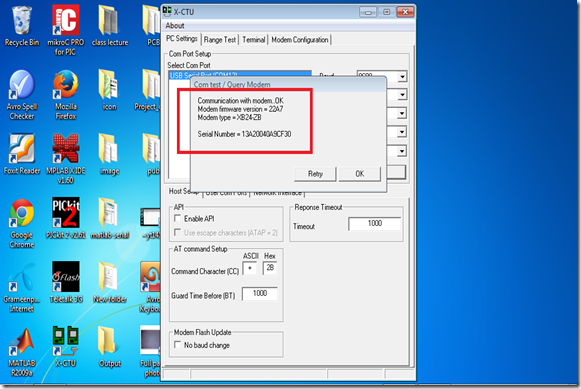
xbee2

Look at the serial number . It is important because you have to give this number in software later, so save it somewhere else. Click OK.
During my first try I made mistake in connection. So it shows

xbee

So if you see this message don’t be afraid,check the connection,may be there is a silly mistake somewhere.
Then go to modem configuration(these button stays at the top menu of the software).Click Read Button.Then it will show the parameters of your Xbee module.

xbee3

Now it is time to configure it as a coordinator or router. Here we configured as router.
Choose the function set as ZIGBEE ROUTER AT.
Choose a PAN ID between 0000 to FFFF. Here I choose 2001.

xbee

Next give Destination Address High and Destination Address Low from the serial number. My XBee module serial no. was 0013A20040A9CF4E. So I set Destination Address High as 0013A200.

xbee

Then I set Destination Address Low as 40A9CF4E.

xbee

Then click the read button. And you are done.

IMG_20140223_130840_1
Read More..

Wednesday, September 10, 2014

60W Power Audio Amplifier with 2N3055

This schema is simple and inexpensive:

60W


This is a class B amplifier, this means, that a current must flow through the end transistors, even if there is no signal on the input. This current can be regulated with the 500Ω trimmer resistor. As this current incrases, the sound of the amplifier gets better, but the end transistors are more heating. But if this current decrases, the transistors are not heating so much, but the sound gets worse.

you can download the document version here
Read More..

Tuesday, September 9, 2014

TDA1556Q 2 x 22 W stereo BTL differential amplifier with speaker protection

FEATURES

Few peripheral components
High output power
Low output offset voltage
Fixed gain
Loudspeaker protection (with diagnostic facility)
Differential inputs
Dynamic Distortion Detector (DDD)
High common mode input signal
Very high CMRR
Good ripple rejection
Mute/stand-by switch
Load dump protection
Short-circuit safe
Thermally protected
Reverse polarity safe
High energy handling capability at the outputs (VP = 0 V)
Electrostatic discharge protection
No switch-on/switch-off plop
Flexible leads
Low thermal resistance

GENERAL DESCRIPTION

TDA1556Q is a monolithic integrated class-B output amplifier containing two 22 Watt amplifiers in a BTL configuration. The device is contained in a 17-lead single-in-line (SIL) plastic power package. It has two differential inputs and is primarily intended for car booster applications.

Circuit Diagram:
Circuit diagram for TDA1556Q 2 x 22 W stereo BTL differential amplifier with speaker protection

Read More..

Monday, September 8, 2014

Inverter 5000W with PWM Pulse Width Modulator

Inverter 5000W with PWM
Inverter

This inverter uses PWM (Pulse Width Modulator) with type IC SG3524. IC serves as a oscillator 50Hz, as a regulator of the desired output voltage. Input power ranging from 250W up to 5000W output and has. Following a series INVERTER 5000W with PWM (Pulse Width Modulator).


Inverter
Schematic Inverter 5000W with PWM (Pulse Width Modulator)

Inverter
Layout PCB Inverter 5000W with PWM (Pulse Width Modulator)

below is the output power settings that can be issued by this inverter:
DC voltage and Transformer "T2" winding recommendation:
Winding Power Supply
12VDC 750W P: 24V "12-0-12" / S: 220V
1500W 24VDC P: 48V "24-0-24" / S: 220V
2250w 36VDC P: 72V "36-0-36" / S: 220V
3000w 48VDC P: 96V "48-0-48" / S: 220V
3750w 60VDC P: 120V "60-0-60" / S: 220V
4500w 72VDC P: 144V "72-0-72" / S: 220V
5250w 84VDC P: 168V "84-0-84" / S: 220V

Transformer used is the transformer CT
R1 serves to regulate the voltage to 220v inverter
R2 serves to regulate the inverter output frequency of 50 or 60 Hz (as appropriate)


power
Read More..

Sunday, September 7, 2014

Low cost Step down Converter with Wide Input Voltage Range

The schema described here is mostly aimed at development engineers who are looking for an economical step-down converter which offers a wide input volt- age range. As a rule this type of schema employs a step-down converter with integrated switching element. However, by using a more discrete solution it is possible to reduce the total cost of the step- down converter, especially when manufacturing in quantity. The TL5001A is a low-cost PWM controller which is ideal for this project. The input voltage range for the step-down converter described here is from 8 V to 30 V, with an output voltage of 5 V and a maximum output current of 1.5 A. When the input voltage is applied the PWM output of IC1 is enabled, taking one end of the voltage divider formed by R1 and R2 to ground potential. The cur-rent through the voltage divider will then be at most 25 mA: this value is obtained by dividing the maximum input voltage (30 V) minus the saturation voltage of the output driver (2 V) by the total resistance of the voltage divider (1.1 kΩ ). T1 and T3 together form an NPN/PNP driver stage to charge the gate capacitance of P-channel MOSFET T2 as quickly as possible, and then, at the turn-off point, discharge it again. The base-emitter junction of T3 goes into a conducting state when the PWM output is active and a voltage is dropped across R2. T3 will then also conduct from collector to emitter and the gate capacitance of T2 will be discharged down to about 800 mV. The P-channel MOSFET will then conduct from drain to source. If the open-collector output of the controller is deactivated, a negligibly small current flows through resistor R2 and the base of T1 will be raised to the input voltage level. The base-emitter junction of T1 will then conduct and the gate capacitance of T2 will be charged up to the input voltage level through the collector and emitter of T1. The P-channel MOSFET will then no longer conduct from drain to source. This driver schema constructed from discrete components is very fast, giving very quick switch-over times. Diodes D2 and D3 provide voltage limiting for the P-channel MOSFET, whose maximum gate-source voltage is 20 V. If the Zener voltage of diode D2 is exceeded it starts to conduct; when the forward voltage of diode D3 is also exceeded, the two diodes together clamp the gate-source voltage to approximately 19 V. The switching frequency is set at approximately 100 kHz, which gives a good compromise between efficiency and component size. Finally, a few notes on component selection. All resistors are 1/16 W, 1 %. Apart from electrolytic C1 all the capacitors are ceramic types. For the two larger values (C2 and C5) the following are used: C2 is a Murata type GRM21BR71C105KA01 ceramic capacitor, 1 µF, 16 V, X7R, 10 %; C5 is a Murata type GRM32ER60J476ME20 ceramic capacitor, 47 µF,  6.3 V, X5R, 10 %. D1 (Fairchild type MBRS340T3) is a 40 V/3 A Schottky diode. Coil L1 is a Würth WE-PD power choke type 744771147, 47 µH, 2.21 A, 75 mΩ. T1 (BC846) and T3 (BC856) are 60 V, 200 mA, 310 mW complementary bipolar transistors from Vishay. The TL5001AID (IC1) is a low-cost PWM controller with an open-collector output from Texas Instruments.

Author : Dirk Gehrke Copyright : Elektor

Read More..